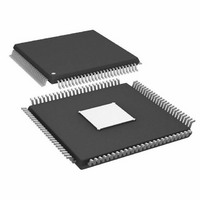
AD9910BSVZ-REEL Analog Devices Inc, AD9910BSVZ-REEL Datasheet - Page 44

AD9910BSVZ-REEL
Manufacturer Part Number
AD9910BSVZ-REEL
Description
IC,FREQUENCY SYNTHESIZER,CMOS,TQFP,100PIN,PLASTIC
Manufacturer
Analog Devices Inc
Datasheet
1.AD9910BSVZ-REEL.pdf
(64 pages)
Specifications of AD9910BSVZ-REEL
Design Resources
Synchronizing Multiple AD9910 1 GSPS Direct Digital Synthesizers (CN0121)
Resolution (bits)
14 b
Master Fclk
1GHz
Tuning Word Width (bits)
32 b
Voltage - Supply
1.8V, 3.3V
Operating Temperature
-40°C ~ 85°C
Mounting Type
Surface Mount
Package / Case
100-TQFP Exposed Pad, 100-eTQFP, 100-HTQFP, 100-VQFP
Lead Free Status / RoHS Status
Lead free / RoHS Compliant
For Use With
AD9910/PCBZ - BOARD EVAL FOR AD9910 1GSPS
Lead Free Status / RoHS Status
Lead free / RoHS Compliant
Available stocks
Company
Part Number
Manufacturer
Quantity
Price
Company:
Part Number:
AD9910BSVZ-REEL
Manufacturer:
Analog Devices Inc
Quantity:
10 000
AD9910
SYNCHRONIZATION OF MULTIPLE DEVICES
Multiple devices are synchronized when their clock states match
and they transition between states simultaneously. Clock
synchronization allows the user to asynchronously program
multiple devices but synchronously activate the programming by
applying a coincident I/O update to all devices
The function of the synchronization logic in the AD9910 is to
force the internal clock generator to a predefined state coincident
with an external synchronization signal applied to the SYNC_INx
pins. If all devices are forced to the same clock state in synchro-
nization with the same external signal, then the devices are, by
definition, synchronized. Figure 50 is a block diagram of the
synchronization function. The synchronization logic is divided
into two independent blocks: a sync generator and a sync receiver,
both of which use the local SYSCLK signal for internal timing.
The synchronization mechanism relies on the premise that the
REFCLK signal appearing at each device is edge aligned with all
others as a result of the external REFCLK distribution system
(see Figure 53).
INTERNAL
CLOCKS
Figure 50. Synchronization Circuit Block Diagram
RECEIVER
SYNC
VALIDATION
HOLD VALIDATION
DELAY
SYNC
SYSCLK
RECEIVER
ENABLE
SYNC
SETUP AND
GENERATOR
4
INPUT DELAY
DETECTION
AND EDGE
SYNC
VALIDATION
CIRCUITRY
REF_CLK
DISABLE
TIMING
INPUT
SYNC
RECEIVER
DELAY
SYNC
5
5
90
91
10
12
9
7
8
REF_CLK
REF_CLK
SYNC_OUT+
SYNC_OUT–
SYNC_IN+
SYNC_IN–
SYNC_SMP_ERR
Rev. C | Page 44 of 64
The sync generator block is shown in Figure 51. It is activated
via the sync generator enable bit. It allows for one AD9910 in a
group to function as a master timing source with the remaining
devices slaved to the master.
The sync generator produces a clock signal that appears at the
SYNC_OUTx pins. This clock is delivered by an LVDS driver
and exhibits a 50% duty cycle. The clock has a fixed frequency
given by
The clock at the SYNC_OUTx pins synchronizes with either the
rising or falling edge of the internal SYSCLK signal, as determined
by the sync generator polarity bit. Because the SYNC_OUTx signal
is synchronized with the internal SYSCLK of the master device,
the master device SYSCLK serves as the reference timing source
for all slave devices. The user can adjust the output delay of the
SYNC_OUTx signal in steps of ~150 ps by programming the 5-bit
output sync generator delay word via the serial I/O port. The
programmable output delay facilitates added edge timing
flexibility to the overall synchronization mechanism.
The sync receiver block (shown in Figure 52) is activated via the
sync receiver enable bit (0x0A[27]). The sync receiver consists
of three subsections: the input delay and edge detection block,
the internal clock generator block, and the setup and hold
validation block.
The clock generator block remains operational even if the sync
receiver is not enabled.
SYSCLK
f
SYNC
POLARITY
_
OUT
SYNC
=
Figure 51. Sync Generator Diagram
f
÷16
0
1
SYSCLK
16
GENERATOR
ENABLE
SYNC
D Q
R
PROGAMMABLE
GENERATOR
DELAY
DELAY
SYNC
5
DRIVER
LVDS
10
10
9
9
SYNC_OUT+
SYNC_OUT–


