AD9910BSVZ-REEL Analog Devices Inc, AD9910BSVZ-REEL Datasheet - Page 19
AD9910BSVZ-REEL
Manufacturer Part Number
AD9910BSVZ-REEL
Description
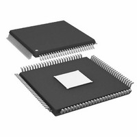
IC,FREQUENCY SYNTHESIZER,CMOS,TQFP,100PIN,PLASTIC
Manufacturer
Analog Devices Inc
Datasheet
1.AD9910BSVZ-REEL.pdf
(64 pages)
Specifications of AD9910BSVZ-REEL
Design Resources
Synchronizing Multiple AD9910 1 GSPS Direct Digital Synthesizers (CN0121)
Resolution (bits)
14 b
Master Fclk
1GHz
Tuning Word Width (bits)
32 b
Voltage - Supply
1.8V, 3.3V
Operating Temperature
-40°C ~ 85°C
Mounting Type
Surface Mount
Package / Case
100-TQFP Exposed Pad, 100-eTQFP, 100-HTQFP, 100-VQFP
Lead Free Status / RoHS Status
Lead free / RoHS Compliant
For Use With
AD9910/PCBZ - BOARD EVAL FOR AD9910 1GSPS
Lead Free Status / RoHS Status
Lead free / RoHS Compliant
Available stocks
Company
Part Number
Manufacturer
Quantity
Price
Company:

Part Number:
AD9910BSVZ-REEL
Manufacturer:
Analog Devices Inc
Quantity:
10 000


DIGITAL RAMP MODULATION MODE
In digital ramp modulation mode (see Figure 24), the modulated
DDS signal control parameter is supplied directly from the
digital ramp generator (DRG). The ramp generation parameters
are controlled through the serial I/O port.
The ramp generation parameters allow the user to control both
the rising and falling slopes of the ramp. The upper and lower
boundaries of the ramp, the step size and step rate of the rising
portion of the ramp, and the step size and step rate of the falling
portion of the ramp are all programmable.
PROFILE[2:0]
I/O_UPDATE
TxENABLE
I/O_RESET
PARALLEL
DRHOLD
DROVER
PDCLK
DRCTL
INPUT
SCLK
SDIO
OSK
CS
16
2
2
2
3
PARALLEL DATA
TIMING AND
CONTROL
PROGRAMMING
REGISTERS
8
RAM_SWP_OVR
GENERATOR
DAC FSC
OUTPUT
KEYING
DIGITAL
SHIFT
RAMP
RAM
PARTITION
CONTROL
ROUTE
DATA
AND
Figure 24. Digital Ramp Modulation Mode
AMPLITUDE (A)
PHASE (θ)
FREQUENCY (ω)
Rev. C | Page 19 of 64
INTERNAL CLOCK TIMING
AND CONTROL
AD9910
CONTROL
POWER-
DOWN
CLOCK
A
ω
θ
DDS
The ramp is digitally generated with 32-bit output resolution.
The 32-bit output of the DRG can be programmed to represent
frequency, phase, or amplitude. When programmed to represent
frequency, all 32 bits are used. However, when programmed to
represent phase or amplitude, only the 16 MSBs or 14 MSBs,
respectively, are used.
The ramp direction (rising or falling) is externally controlled by
the DRCTL pin. An additional pin (DRHOLD) allows the user
to suspend the ramp generator in its present state.
Asin (ωt + θ)
Acos (ωt + θ)
SYNCHRONIZATION
MULTICHIP
SYSCLK
DAC FSC
2
2
INVERSE
FILTER
SINC
8
PLL
÷2
8-BIT
AUX
DAC
14-BIT
DAC
DAC_RSET
IOUT
IOUT
REFCLK_OUT
REF_CLK
REF_CLK
XTAL_SEL
AD9910
Related parts for AD9910BSVZ-REEL
Image
Part Number
Description
Manufacturer
Datasheet
Request
R

Part Number:
Description:
Direct Digital Synthesis Evaluation Board
Manufacturer:
Analog Devices Inc
Datasheet:

Part Number:
Description:
3.3V CMOS Direct Digital Synthesizer
Manufacturer:
Analog Devices
Datasheet:

Part Number:
Description:
±1.7g Dual-Axis IMEMS Accelerometer Evaluation Board
Manufacturer:
Analog Devices Inc
Datasheet:

Part Number:
Description:
Inertial Sensor Evaluation System
Manufacturer:
Analog Devices Inc
Datasheet:
Part Number:
Description:
Manufacturer:
Analog Devices Inc
Datasheet:
Part Number:
Description:
Manufacturer:
Analog Devices Inc
Datasheet:
Part Number:
Description:
Manufacturer:
Analog Devices Inc
Datasheet:
Part Number:
Description:
Manufacturer:
Analog Devices Inc
Datasheet:
Part Number:
Description:
Manufacturer:
Analog Devices Inc
Datasheet:
Part Number:
Description:
Manufacturer:
Analog Devices Inc
Datasheet:
Part Number:
Description:
Manufacturer:
Analog Devices Inc
Datasheet:
Part Number:
Description:
Manufacturer:
Analog Devices Inc
Datasheet:
Part Number:
Description:
Manufacturer:
Analog Devices Inc
Datasheet: