AD9910BSVZ-REEL Analog Devices Inc, AD9910BSVZ-REEL Datasheet - Page 61
AD9910BSVZ-REEL
Manufacturer Part Number
AD9910BSVZ-REEL
Description
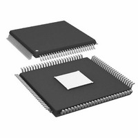
IC,FREQUENCY SYNTHESIZER,CMOS,TQFP,100PIN,PLASTIC
Manufacturer
Analog Devices Inc
Datasheet
1.AD9910BSVZ-REEL.pdf
(64 pages)
Specifications of AD9910BSVZ-REEL
Design Resources
Synchronizing Multiple AD9910 1 GSPS Direct Digital Synthesizers (CN0121)
Resolution (bits)
14 b
Master Fclk
1GHz
Tuning Word Width (bits)
32 b
Voltage - Supply
1.8V, 3.3V
Operating Temperature
-40°C ~ 85°C
Mounting Type
Surface Mount
Package / Case
100-TQFP Exposed Pad, 100-eTQFP, 100-HTQFP, 100-VQFP
Lead Free Status / RoHS Status
Lead free / RoHS Compliant
For Use With
AD9910/PCBZ - BOARD EVAL FOR AD9910 1GSPS
Lead Free Status / RoHS Status
Lead free / RoHS Compliant
Available stocks
Company
Part Number
Manufacturer
Quantity
Price
Company:

Part Number:
AD9910BSVZ-REEL
Manufacturer:
Analog Devices Inc
Quantity:
10 000


Profile Registers
There are eight consecutive serial I/O addresses (Address 0x0E
to Address 0x015) dedicated to device profiles. All eight profile
registers are either single tone profiles or RAM profiles. RAM
profiles are in effect when CFR1[31] = 1. Single tone profiles are
in effect when CFR1[31] = 0, CFR2[19] = 0, and CFR2[4] = 0.
Profile 0 to Profile 7, Single Tone Registers—Address 0x0E to Address 0x15
Eight bytes are assigned to each register.
Table 30. Bit Descriptions for Profile 0 to Profile 7 Single Tone Register
Bit(s)
63:62
61:48
47:32
31:0
RAM Profile 0 to RAM Profile 7, Control Registers—Address 0x0E to Address 0x15
Eight bytes are assigned to each register.
Table 31. Bit Descriptions for Profile 0 to Profile 7 RAM Register
Bit(s)
63:56
55:40
39:30
29:24
23:14
13:6
5
4
3
2:0
RAM Register—Address 0x16
Four bytes are assigned to the RAM register.
Table 32. Bit Descriptions for RAM Register
Bit(s)
31:0
Mnemonic
Open
Amplitude scale factor
Phase offset word
Frequency tuning word
Mnemonic
Open
Address step rate
Waveform end address
Open
Waveform start address
Open
No-dwell high
Open
Zero-crossing
RAM mode control
Mnemonic
RAM word
Description
This 14-bit number controls the DDS output amplitude.
This 16-bit number controls the DDS phase offset.
This 32-bit number controls the DDS frequency.
Description
16-bit address step rate value.
10-bit waveform end address.
10-bit waveform start address.
Effective only when the RAM mode is in ramp-up.
Effective only when in RAM mode, direct switch.
See Table 13 for details.
Description
The start and end addresses in the RAM Profile 0 to RAM Profile 7 control registers define
the number of 32-bit words (1 minimum, 1024 maximum) to be written to the RAM register.
0 = when the RAM state machine reaches the end address, it halts.
1 = when the RAM state machines reaches the end address, it jumps to the start address
and halts.
0 = zero-crossing function disabled.
1 = zero-crossing function enabled.
Rev. C | Page 61 of 64
In normal operation, the active profile register is selected using
the external PROFILE[2:0] pins. However, in the specific case
when CFR1[31] = 1 and CFR1[20:17] ≠ 0000b, the active profile
is selected automatically (see the RAM Ramp-Up Internal
Profile Control Mode section).
AD9910
Related parts for AD9910BSVZ-REEL
Image
Part Number
Description
Manufacturer
Datasheet
Request
R

Part Number:
Description:
Direct Digital Synthesis Evaluation Board
Manufacturer:
Analog Devices Inc
Datasheet:

Part Number:
Description:
3.3V CMOS Direct Digital Synthesizer
Manufacturer:
Analog Devices
Datasheet:

Part Number:
Description:
±1.7g Dual-Axis IMEMS Accelerometer Evaluation Board
Manufacturer:
Analog Devices Inc
Datasheet:

Part Number:
Description:
Inertial Sensor Evaluation System
Manufacturer:
Analog Devices Inc
Datasheet:
Part Number:
Description:
Manufacturer:
Analog Devices Inc
Datasheet:
Part Number:
Description:
Manufacturer:
Analog Devices Inc
Datasheet:
Part Number:
Description:
Manufacturer:
Analog Devices Inc
Datasheet:
Part Number:
Description:
Manufacturer:
Analog Devices Inc
Datasheet:
Part Number:
Description:
Manufacturer:
Analog Devices Inc
Datasheet:
Part Number:
Description:
Manufacturer:
Analog Devices Inc
Datasheet:
Part Number:
Description:
Manufacturer:
Analog Devices Inc
Datasheet:
Part Number:
Description:
Manufacturer:
Analog Devices Inc
Datasheet:
Part Number:
Description:
Manufacturer:
Analog Devices Inc
Datasheet: