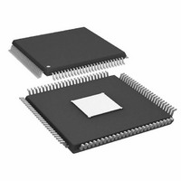
AD9910BSVZ-REEL Analog Devices Inc, AD9910BSVZ-REEL Datasheet - Page 45

AD9910BSVZ-REEL
Manufacturer Part Number
AD9910BSVZ-REEL
Description
IC,FREQUENCY SYNTHESIZER,CMOS,TQFP,100PIN,PLASTIC
Manufacturer
Analog Devices Inc
Datasheet
1.AD9910BSVZ-REEL.pdf
(64 pages)
Specifications of AD9910BSVZ-REEL
Design Resources
Synchronizing Multiple AD9910 1 GSPS Direct Digital Synthesizers (CN0121)
Resolution (bits)
14 b
Master Fclk
1GHz
Tuning Word Width (bits)
32 b
Voltage - Supply
1.8V, 3.3V
Operating Temperature
-40°C ~ 85°C
Mounting Type
Surface Mount
Package / Case
100-TQFP Exposed Pad, 100-eTQFP, 100-HTQFP, 100-VQFP
Lead Free Status / RoHS Status
Lead free / RoHS Compliant
For Use With
AD9910/PCBZ - BOARD EVAL FOR AD9910 1GSPS
Lead Free Status / RoHS Status
Lead free / RoHS Compliant
Available stocks
Company
Part Number
Manufacturer
Quantity
Price
Company:
Part Number:
AD9910BSVZ-REEL
Manufacturer:
Analog Devices Inc
Quantity:
10 000
The sync receiver accepts a periodic clock signal at the SYNC_
INx pins. This signal is assumed to originate from an LVDS-
compatible driver. The user can delay the SYNC_INx signal in
steps of ~150 ps by programming the 5-bit input sync receiver
delay word in the multichip sync register. The signal at the
output of the programmable delay is referred to as the delayed
SYNC_INx signal.
The edge detection logic generates a sync pulse having a dura-
tion of one SYSCLK cycle with a repetition rate equal to the
frequency of the signal applied to the SYNC_INx pins. The
sync pulse is generated as a result of sampling the rising edge
of the delayed SYNC_INx signal with the rising edge of the
local SYSCLK. The sync pulse is routed to the internal clock
generator, which behaves as a presettable counter clocked at the
SYNC_SMP_ERR
SYNC_IN+
SYNC_IN–
AT REF_CLK
ALIGNED
INPUTS
EDGE
12
7
8
VALIDATION
RECEIVER
FPGA
FPGA
FPGA
LVDS
DISABLE
DELAYED SYNC-IN SIGNAL
TIMING
SYNC
DELAY EQUALIZATION
CLOCK DISTRIBUTION
SETUP AND HOLD
(FOR EXAMPLE AD951x)
Figure 53. Multichip Synchronization Example
VALIDATION
PROGAMMABLE
AND
Figure 52. Sync Receiver Diagram
DELAY
RECEIVER
DATA
DATA
DATA
DELAY
SYNC
SYNC
VALIDATION
DELAY
Rev. C | Page 45 of 64
4
5
SYNC
SYNC
SYNC
NUMBER 1
NUMBER 2
NUMBER 3
AD9910
AD9910
AD9910
IN
IN
IN
REF_CLK
REF_CLK
REF_CLK
SOURCE
CLOCK
RISING EDGE
GENERATOR
DETECTOR
RECEIVER
SYNC
SYNC
SYNC
ENABLE
STROBE
OUT
OUT
OUT
SYNC
SYSCLK rate. The sync pulse presets the counter to a predefined
state (programmable via the 6-bit sync state preset value word
in the multichip sync register). The predefined state is only active
for a single SYSCLK cycle, after which the clock generator resumes
cycling through its state sequence at the SYSCLK rate. This
unique state presetting mechanism gives the user the flexibility
to synchronize devices with specific relative clock state offsets
(by assigning a different sync state preset value word to each
device).
Multiple device synchronization is accomplished by providing
each AD9910 with a SYNC_INx signal that is edge aligned
across all the devices. If the SYNC_INx signal is edge aligned at all
devices, and all devices have the same sync receiver delay and
sync state preset value, then they all have matching clock states
AND
SYNC PULSE
MASTER DEVICE
AT SYNC_IN
ALIGNED
INPUTS.
EDGE
DELAY EQUALIZATION
(FOR EXAMPLE AD951x)
SYNCHRONIZATION
DISTRIBUTION AND
GENERATOR
RESET
CLOCK
Q0
Qn
•
•
•
•
•
•
CLOCK
STATE
INTERNAL
CLOCKS
SYSCLK
AD9910


