AD9910BSVZ-REEL Analog Devices Inc, AD9910BSVZ-REEL Datasheet - Page 18
AD9910BSVZ-REEL
Manufacturer Part Number
AD9910BSVZ-REEL
Description
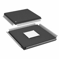
IC,FREQUENCY SYNTHESIZER,CMOS,TQFP,100PIN,PLASTIC
Manufacturer
Analog Devices Inc
Datasheet
1.AD9910BSVZ-REEL.pdf
(64 pages)
Specifications of AD9910BSVZ-REEL
Design Resources
Synchronizing Multiple AD9910 1 GSPS Direct Digital Synthesizers (CN0121)
Resolution (bits)
14 b
Master Fclk
1GHz
Tuning Word Width (bits)
32 b
Voltage - Supply
1.8V, 3.3V
Operating Temperature
-40°C ~ 85°C
Mounting Type
Surface Mount
Package / Case
100-TQFP Exposed Pad, 100-eTQFP, 100-HTQFP, 100-VQFP
Lead Free Status / RoHS Status
Lead free / RoHS Compliant
For Use With
AD9910/PCBZ - BOARD EVAL FOR AD9910 1GSPS
Lead Free Status / RoHS Status
Lead free / RoHS Compliant
Available stocks
Company
Part Number
Manufacturer
Quantity
Price
Company:

Part Number:
AD9910BSVZ-REEL
Manufacturer:
Analog Devices Inc
Quantity:
10 000


AD9910
RAM MODULATION MODE
The RAM modulation mode (see Figure 23) is activated via the
RAM enable bit and assertion of the I/O_UPDATE pin (or a
profile change). In this mode, the modulated DDS signal control
parameters are supplied directly from RAM.
The RAM consists of 32-bit words and is 1024 words deep.
Coupled with a sophisticated internal state machine, the RAM
provides a very flexible method for generating arbitrary, time
dependent waveforms. A programmable timer controls the rate
at which words are extracted from the RAM for delivery to the
DDS. Thus, the programmable timer establishes a sample rate at
which 32-bit samples are supplied to the DDS.
PROFILE[2:0]
I/O_UPDATE
I/O_RESET
PARALLEL
TxENABLE
DRHOLD
DROVER
PDCLK
DRCTL
INPUT
SCLK
SDIO
OSK
CS
16
2
2
2
3
PARALLEL DATA
TIMING AND
CONTROL
PROGRAMMING
REGISTERS
8
RAM_SWP_OVR
GENERATOR
DAC FSC
OUTPUT
KEYING
DIGITAL
SHIFT
RAMP
RAM
PARTITION
CONTROL
ROUTE
DATA
AND
Figure 23. RAM Modulation Mode
AMPLITUDE (A)
PHASE (θ)
FREQUENCY (ω)
Rev. C | Page 18 of 64
INTERNAL CLOCK TIMING
AND CONTROL
AD9910
CONTROL
POWER-
DOWN
CLOCK
ω
A
θ
DDS
The selection of the specific DDS signal control parameters that
serve as the destination for the RAM samples is also programmable
through eight independent RAM profile registers. Select a par-
ticular profile using the three external profile pins (PROFILE[2:0]).
A change in the state of the profile pins with the next rising
edge on SYNC_CLK activates the selected RAM profile.
In RAM modulation mode, the ability to generate a time depen-
dent amplitude, phase, or frequency signal enables modulation
of any one of the parameters controlling the DDS carrier signal.
Furthermore, a polar modulation format is available that partitions
each RAM sample into a magnitude and phase component; 16 bits
are allocated to phase and 14 bits are allocated to magnitude.
Acos (ωt + θ)
Asin (ωt + θ)
SYNCHRONIZATION
MULTICHIP
SYSCLK
DAC FSC
2
2
INVERSE
FILTER
SINC
8
PLL
÷2
8-BIT
AUX
DAC
14-BIT
DAC
DAC_RSET
IOUT
IOUT
REFCLK_OUT
REF_CLK
REF_CLK
XTAL_SEL
Related parts for AD9910BSVZ-REEL
Image
Part Number
Description
Manufacturer
Datasheet
Request
R

Part Number:
Description:
Direct Digital Synthesis Evaluation Board
Manufacturer:
Analog Devices Inc
Datasheet:

Part Number:
Description:
3.3V CMOS Direct Digital Synthesizer
Manufacturer:
Analog Devices
Datasheet:

Part Number:
Description:
±1.7g Dual-Axis IMEMS Accelerometer Evaluation Board
Manufacturer:
Analog Devices Inc
Datasheet:

Part Number:
Description:
Inertial Sensor Evaluation System
Manufacturer:
Analog Devices Inc
Datasheet:
Part Number:
Description:
Manufacturer:
Analog Devices Inc
Datasheet:
Part Number:
Description:
Manufacturer:
Analog Devices Inc
Datasheet:
Part Number:
Description:
Manufacturer:
Analog Devices Inc
Datasheet:
Part Number:
Description:
Manufacturer:
Analog Devices Inc
Datasheet:
Part Number:
Description:
Manufacturer:
Analog Devices Inc
Datasheet:
Part Number:
Description:
Manufacturer:
Analog Devices Inc
Datasheet:
Part Number:
Description:
Manufacturer:
Analog Devices Inc
Datasheet:
Part Number:
Description:
Manufacturer:
Analog Devices Inc
Datasheet:
Part Number:
Description:
Manufacturer:
Analog Devices Inc
Datasheet: