C8051F206DK-G Silicon Laboratories Inc, C8051F206DK-G Datasheet - Page 67
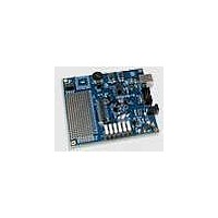
C8051F206DK-G
Manufacturer Part Number
C8051F206DK-G
Description
MCU, MPU & DSP Development Tools MCU DEVELOPMENT KIT W/ GLOBAL POWER SPLY
Manufacturer
Silicon Laboratories Inc
Datasheet
1.C8051F226DK.pdf
(146 pages)
Specifications of C8051F206DK-G
Processor To Be Evaluated
C8051F206
Data Bus Width
8 bit
Interface Type
USB
Lead Free Status / RoHS Status
Lead free / RoHS Compliant


C8051F2xx
9.2.5. Stack
A programmer's stack can be located anywhere in the 256-byte data memory. The stack area is desig-
nated using the Stack Pointer (SP, 0x81) SFR. The SP will point to the last location used. The next value
pushed on the stack is placed at SP+1 and then SP is incremented. A reset initializes the stack pointer to
location 0x07. Therefore, the first value pushed on the stack is placed at location 0x08, which is also the
first register (R0) of register bank 1. Thus, if more than one register bank is to be used, the SP should be
initialized to a location in the data memory not being used for data storage. The stack depth can extend up
to 256 bytes.
The MCU also has built-in hardware for a stack record. The stack record is a 32-bit shift register, where
each Push or increment SP pushes one record bit onto the register, and each Call pushes two record bits
onto the register. (A Pop or decrement SP pops one record bit, and a Return pops two record bits, also.)
The stack record circuitry can also detect an overflow or underflow on the 32-bit shift register, and can
notify the emulator software even with the MCU running full-speed debug.
Rev. 1.6
67
Related parts for C8051F206DK-G
Image
Part Number
Description
Manufacturer
Datasheet
Request
R

Part Number:
Description:
SMD/C°/SINGLE-ENDED OUTPUT SILICON OSCILLATOR
Manufacturer:
Silicon Laboratories Inc
Part Number:
Description:
Manufacturer:
Silicon Laboratories Inc
Datasheet:
Part Number:
Description:
N/A N/A/SI4010 AES KEYFOB DEMO WITH LCD RX
Manufacturer:
Silicon Laboratories Inc
Datasheet:
Part Number:
Description:
N/A N/A/SI4010 SIMPLIFIED KEY FOB DEMO WITH LED RX
Manufacturer:
Silicon Laboratories Inc
Datasheet:
Part Number:
Description:
N/A/-40 TO 85 OC/EZLINK MODULE; F930/4432 HIGH BAND (REV E/B1)
Manufacturer:
Silicon Laboratories Inc
Part Number:
Description:
EZLink Module; F930/4432 Low Band (rev e/B1)
Manufacturer:
Silicon Laboratories Inc
Part Number:
Description:
I°/4460 10 DBM RADIO TEST CARD 434 MHZ
Manufacturer:
Silicon Laboratories Inc
Part Number:
Description:
I°/4461 14 DBM RADIO TEST CARD 868 MHZ
Manufacturer:
Silicon Laboratories Inc
Part Number:
Description:
I°/4463 20 DBM RFSWITCH RADIO TEST CARD 460 MHZ
Manufacturer:
Silicon Laboratories Inc
Part Number:
Description:
I°/4463 20 DBM RADIO TEST CARD 868 MHZ
Manufacturer:
Silicon Laboratories Inc
Part Number:
Description:
I°/4463 27 DBM RADIO TEST CARD 868 MHZ
Manufacturer:
Silicon Laboratories Inc
Part Number:
Description:
I°/4463 SKYWORKS 30 DBM RADIO TEST CARD 915 MHZ
Manufacturer:
Silicon Laboratories Inc
Part Number:
Description:
N/A N/A/-40 TO 85 OC/4463 RFMD 30 DBM RADIO TEST CARD 915 MHZ
Manufacturer:
Silicon Laboratories Inc
Part Number:
Description:
I°/4463 20 DBM RADIO TEST CARD 169 MHZ
Manufacturer:
Silicon Laboratories Inc