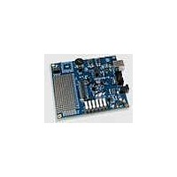
C8051F206DK-G Silicon Laboratories Inc, C8051F206DK-G Datasheet - Page 106

C8051F206DK-G
Manufacturer Part Number
C8051F206DK-G
Description
MCU, MPU & DSP Development Tools MCU DEVELOPMENT KIT W/ GLOBAL POWER SPLY
Manufacturer
Silicon Laboratories Inc
Datasheet
1.C8051F226DK.pdf
(146 pages)
Specifications of C8051F206DK-G
Processor To Be Evaluated
C8051F206
Data Bus Width
8 bit
Interface Type
USB
Lead Free Status / RoHS Status
Lead free / RoHS Compliant
- Current page: 106 of 146
- Download datasheet (2Mb)
C8051F2xx
106
Bits7–0: Port0 Digital/Analog Input Mode
Bits7–0: P1.[7:0]
Bits7–0: PRT1CF.[7:0]: Output Configuration Bits for P1.7–P1.0 (respectively)
P1.7
R/W
Bit7
R/W
Bit7
R/W
Bit7
0: Corresponding Port0 pin Digital Input disabled. (For analog use, i.e., ADC).
1: Corresponding Port0 pin Digital Input is enabled.
(Write - Output appears on I/O pins per PRT0MX, PRT1MX, and PRT2MX registers)
0: Logic Low Output.
1: Logic High Output (high impedance if corresponding PRT1CF.n bit = 0)
(Read - Regardless of PRT0MX, PRT1MX, and PRT2MX Register settings).
0: P1.n pin is logic low.
1: P1.n pin is logic high.
0: Corresponding P1.n Output Mode is Open-Drain.
1: Corresponding P1.n Output Mode is Push-Pull.
SFR Definition 14.6. P0MODE: Port0 Digital/Analog Input Mode
P1.6
SFR Definition 14.8. PRT1CF: Port1 Configuration Register
R/W
Bit6
R/W
Bit6
R/W
Bit6
P1.5
R/W
R/W
Bit5
Bit5
R/W
SFR Definition 14.7. P1: Port1 Register
Bit5
P1.4
R/W
Bit4
R/W
Bit4
R/W
Bit4
P1.3
R/W
Bit3
Rev. 1.6
R/W
Bit3
R/W
Bit3
P1.2
R/W
Bit2
R/W
Bit2
R/W
Bit2
P1.1
R/W
Bit1
R/W
Bit1
R/W
Bit1
(bit addressable)
P1.0
R/W
Bit0
R/W
Bit0
R/W
Bit0
SFR Address:
SFR Address:
Reset Value
SFR Address:
Reset Value
Reset Value
11111111
11111111
00000000
0xF1
0x90
0xA5
Related parts for C8051F206DK-G
Image
Part Number
Description
Manufacturer
Datasheet
Request
R
Part Number:
Description:
SMD/C°/SINGLE-ENDED OUTPUT SILICON OSCILLATOR
Manufacturer:
Silicon Laboratories Inc
Part Number:
Description:
Manufacturer:
Silicon Laboratories Inc
Datasheet:
Part Number:
Description:
N/A N/A/SI4010 AES KEYFOB DEMO WITH LCD RX
Manufacturer:
Silicon Laboratories Inc
Datasheet:
Part Number:
Description:
N/A N/A/SI4010 SIMPLIFIED KEY FOB DEMO WITH LED RX
Manufacturer:
Silicon Laboratories Inc
Datasheet:
Part Number:
Description:
N/A/-40 TO 85 OC/EZLINK MODULE; F930/4432 HIGH BAND (REV E/B1)
Manufacturer:
Silicon Laboratories Inc
Part Number:
Description:
EZLink Module; F930/4432 Low Band (rev e/B1)
Manufacturer:
Silicon Laboratories Inc
Part Number:
Description:
I°/4460 10 DBM RADIO TEST CARD 434 MHZ
Manufacturer:
Silicon Laboratories Inc
Part Number:
Description:
I°/4461 14 DBM RADIO TEST CARD 868 MHZ
Manufacturer:
Silicon Laboratories Inc
Part Number:
Description:
I°/4463 20 DBM RFSWITCH RADIO TEST CARD 460 MHZ
Manufacturer:
Silicon Laboratories Inc
Part Number:
Description:
I°/4463 20 DBM RADIO TEST CARD 868 MHZ
Manufacturer:
Silicon Laboratories Inc
Part Number:
Description:
I°/4463 27 DBM RADIO TEST CARD 868 MHZ
Manufacturer:
Silicon Laboratories Inc
Part Number:
Description:
I°/4463 SKYWORKS 30 DBM RADIO TEST CARD 915 MHZ
Manufacturer:
Silicon Laboratories Inc
Part Number:
Description:
N/A N/A/-40 TO 85 OC/4463 RFMD 30 DBM RADIO TEST CARD 915 MHZ
Manufacturer:
Silicon Laboratories Inc
Part Number:
Description:
I°/4463 20 DBM RADIO TEST CARD 169 MHZ
Manufacturer:
Silicon Laboratories Inc


