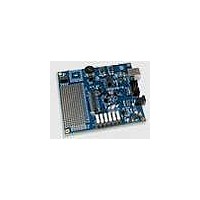
C8051F206DK-G Silicon Laboratories Inc, C8051F206DK-G Datasheet - Page 120

C8051F206DK-G
Manufacturer Part Number
C8051F206DK-G
Description
MCU, MPU & DSP Development Tools MCU DEVELOPMENT KIT W/ GLOBAL POWER SPLY
Manufacturer
Silicon Laboratories Inc
Datasheet
1.C8051F226DK.pdf
(146 pages)
Specifications of C8051F206DK-G
Processor To Be Evaluated
C8051F206
Data Bus Width
8 bit
Interface Type
USB
Lead Free Status / RoHS Status
Lead free / RoHS Compliant
- Current page: 120 of 146
- Download datasheet (2Mb)
C8051F2xx
If T1M (CKCON.4) is logic 1, then the above equation becomes:
If T1M (CKCON.4) is logic 0, then the above equation becomes:
The Timer 2 overflow rate, when in Baud Rate Generator Mode and using an internal clock source, is
determined solely by the Timer 2 16-bit reload value (RCAP2H:RCAP2L). The Timer 2 clock source is
fixed at SYSCLK/2. The Timer 2 overflow rate can be calculated as follows:
Timer 2 can be selected as the baud rate generator for RX and/or TX by setting RCLK (T2CON.5) and/or
TCLK (T2CON.4), respectively. When either RCLK or TCLK is set to logic 1, Timer 2 interrupts are auto-
matically disabled and the timer is forced into Baud Rate Generator Mode with SYSCLK/2 as its clock
source. If a different timebase is required, setting the C/T2 bit (T2CON.1) to logic 1 will allow Timer 2 to be
clocked from the external input pin T2. See the Timers section for complete timer configuration details.
120
Figure 16.5. UART Modes 1, 2, and 3 Interconnect Diagram
T2_OVERFLOWRATE = (SYSCLK/2) / (65536 – [RCAP2H:RCAP2L]).
RS-232
T1_OVERFLOWRATE = (SYSCLK/12) / (256 – TH1).
T1_OVERFLOWRATE = (SYSCLK) / (256 – TH1).
MCU
TX
RX
RS-232
LEVEL
Rev. 1.6
XLTR
OR
RX
RX
TX
TX
C8051Fxxx
C8051Fxxx
Related parts for C8051F206DK-G
Image
Part Number
Description
Manufacturer
Datasheet
Request
R
Part Number:
Description:
SMD/C°/SINGLE-ENDED OUTPUT SILICON OSCILLATOR
Manufacturer:
Silicon Laboratories Inc
Part Number:
Description:
Manufacturer:
Silicon Laboratories Inc
Datasheet:
Part Number:
Description:
N/A N/A/SI4010 AES KEYFOB DEMO WITH LCD RX
Manufacturer:
Silicon Laboratories Inc
Datasheet:
Part Number:
Description:
N/A N/A/SI4010 SIMPLIFIED KEY FOB DEMO WITH LED RX
Manufacturer:
Silicon Laboratories Inc
Datasheet:
Part Number:
Description:
N/A/-40 TO 85 OC/EZLINK MODULE; F930/4432 HIGH BAND (REV E/B1)
Manufacturer:
Silicon Laboratories Inc
Part Number:
Description:
EZLink Module; F930/4432 Low Band (rev e/B1)
Manufacturer:
Silicon Laboratories Inc
Part Number:
Description:
I°/4460 10 DBM RADIO TEST CARD 434 MHZ
Manufacturer:
Silicon Laboratories Inc
Part Number:
Description:
I°/4461 14 DBM RADIO TEST CARD 868 MHZ
Manufacturer:
Silicon Laboratories Inc
Part Number:
Description:
I°/4463 20 DBM RFSWITCH RADIO TEST CARD 460 MHZ
Manufacturer:
Silicon Laboratories Inc
Part Number:
Description:
I°/4463 20 DBM RADIO TEST CARD 868 MHZ
Manufacturer:
Silicon Laboratories Inc
Part Number:
Description:
I°/4463 27 DBM RADIO TEST CARD 868 MHZ
Manufacturer:
Silicon Laboratories Inc
Part Number:
Description:
I°/4463 SKYWORKS 30 DBM RADIO TEST CARD 915 MHZ
Manufacturer:
Silicon Laboratories Inc
Part Number:
Description:
N/A N/A/-40 TO 85 OC/4463 RFMD 30 DBM RADIO TEST CARD 915 MHZ
Manufacturer:
Silicon Laboratories Inc
Part Number:
Description:
I°/4463 20 DBM RADIO TEST CARD 169 MHZ
Manufacturer:
Silicon Laboratories Inc


