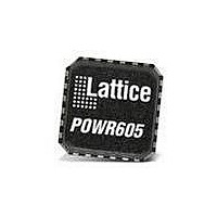
PAC-POWR607-EV Lattice, PAC-POWR607-EV Datasheet - Page 2

PAC-POWR607-EV
Manufacturer Part Number
PAC-POWR607-EV
Description
MCU, MPU & DSP Development Tools ispPAC POWR607 EVAL BRD
Manufacturer
Lattice
Series
ispPAC®r
Specifications of PAC-POWR607-EV
Processor To Be Evaluated
ispPAC-POWR607
Interface Type
JTAG
Maximum Operating Temperature
+ 85 C
Minimum Operating Temperature
- 40 C
Operating Supply Voltage
3.96 V
Core Architecture
CPLD
Main Purpose
Power Management, Power Supply Supervisor/Tracker/Sequencer
Embedded
Yes, Other
Utilized Ic / Part
ispPAC-POWR607
Primary Attributes
-
Secondary Attributes
4.5 ~ 9 V Supply
Lead Free Status / RoHS Status
Lead free / RoHS Compliant
Pin Descriptions
Lattice Semiconductor
and digital inputs used as inputs to the CPLD array. The digital output pins providing the external control signals are
driven by the CPLD. Four independently programmable timers also interface with the CPLD and can create delays
and time-outs ranging from 32µs to 2 seconds. The CPLD is programmed using LogiBuilder™, an easy-to-learn
language integrated into the PAC-Designer
the analog input channel comparators or the digital inputs.
Figure 4-1. ispPAC-POWR607 Block Diagram
Number
11, 12
30
31
27
26
23
22
20
29
IN1_PWRDN
IN_OUT3
IN_OUT4
IN_OUT5
IN_OUT6
IN_OUT7
HVOUT1
HVOUT2
Name
GND
IN1_PWRDN
Ground
Open Drain Output
FET Gate Driver
Open Drain Output
FET Gate Driver
Digital Input
Open Drain Output
Digital Input
Open Drain Output
Digital Input
Open Drain Output
Digital Input
Open Drain Output
Digital Input
Open Drain Output
Digital Input
VMON1
VMON2
VMON3
VMON4
VMON5
VMON6
IN2
Pin Type
9
9
9
9
9
®
Power Down
software. Control sequences are written to monitor the status of any of
4 Timers
Logic
2
2
2
2
2
2
2
Ground
0V to 10V
0V to 9V
0V to 10V
0V to 9V
0V to 5.5V
0V to 5.5V
0V to 5.5V
0V to 5.5V
0V to 5.5V
0V to 5.5V
4-2
VCC
Voltage Range
ispPAC-POWR607
JTAG Interface
16 Macrocells
28 Inputs
PLD
3
Ground
Open-Drain Output 1
High-voltage FET Gate Driver 1
Open-Drain Output 2
High-voltage FET Gate Driver 2
PLD Input 3
Open Drain Output 3
PLD Input 4
Open Drain Output 4
PLD Input 5
Open Drain Output 5
PLD Input 6
Open Drain Output 6
PLD Input 7
Open Drain Output 7
PLD Logic Input 1.
should be pulled down with a 10k Ω resistor.
ispPAC-POWR607 Data Sheet
HVOUT1
HVOUT2
IN_OUT3
IN_OUT4
IN_OUT5
IN_OUT6
IN_OUT7
1
Description
4, 5
When not used, this pin


