DLP-245SX DLP Design Inc, DLP-245SX Datasheet - Page 6
DLP-245SX
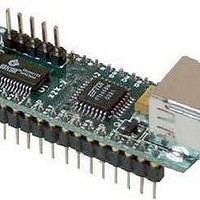
Manufacturer Part Number
DLP-245SX
Description
Interface Modules & Development Tools USB/Micro Dev Board
Manufacturer
DLP Design Inc
Datasheet
1.DLP-245SX.pdf
(14 pages)
Specifications of DLP-245SX
Interface Type
USB
Data Bus Width
8 bit
Operating Supply Voltage
5.25 V
Product
Interface Modules
For Use With/related Products
SX28
Lead Free Status / RoHS Status
Lead free / RoHS Compliant


the drivers (Ftdiunin.exe for VCP and Ftd2xxun.exe for DLL). These uninstall programs are
included with the driver files.
TOKEN I/O
The SX28 microcontroller on the DLP-245SX is shipped from the factory preprogrammed with
firmware that provides rudimentary access to the port pins via either the VCP or DLL drivers.
Features include the ability to read and write individual port pins as well as 8-bit port reads and
writes.
The firmware in the DLP-245SX also provides access to the on-board EEPROM memory, and
communications with digital temperature-sensing devices.
Commands sent to the Token I/O firmware must adhere to a specific communications protocol.
Each command sequence contains the following information:
The checksum is computed by exclusive-OR-ing every byte in the string. If the same checksum
is calculated by the SX28 upon receipt of the packet, then a single-byte reply of 0x55 is returned
to the host. In the event of a checksum error, the SX28 will return an error code of 0xAA. For
example, setting port PIN_A1 high would require the following string of bytes:
0x03, 0xA6, 0x29, 0x01, 0x8D
Definition of the Bytes:
0x03 – Number of bytes in command (checksum excluded)
0xA6 – Command for set port pin high/low
0xA1 – Affected port pin
0x01 – Desired state of port pin
0x8D – Checksum of previous 4 bytes
Byte 0:
Byte 1:
Byte 2…n-1:
Byte n:
Number of bytes in command sequence
Command
Parameter/Data bytes
Checksum
6
Related parts for DLP-245SX
Image
Part Number
Description
Manufacturer
Datasheet
Request
R

Part Number:
Description:
Zigbee / 802.15.4 Modules & Development Tools USE 626-DLP-RF2-Z
Manufacturer:
DLP Design Inc
Datasheet:
Part Number:
Description:
Zigbee / 802.15.4 Modules & Development Tools TTL SERIAL INTERFACE MODULE
Manufacturer:
DLP Design Inc
Datasheet:

Part Number:
Description:
MODULE USB-TO-TTL SRL UART CONV
Manufacturer:
DLP Design Inc
Datasheet:

Part Number:
Description:
Interface Modules & Development Tools FLASH2 TARGET BOARD 18F2321 w/IDE 2k Ltd
Manufacturer:
DLP Design Inc

Part Number:
Description:
Interface Modules & Development Tools FLASH2 TARGET BOARD 16F917 w/IDE 2k Ltd
Manufacturer:
DLP Design Inc

Part Number:
Description:
Interface Modules & Development Tools FLASH2 TARGET BOARD 18F4420 w/IDE 2k Ltd
Manufacturer:
DLP Design Inc
Part Number:
Description:
Zigbee / 802.15.4 Modules & Development Tools TTL SERIAL INTERFACE MODULE
Manufacturer:
DLP Design Inc
Datasheet:

Part Number:
Description:
Interface Modules & Development Tools USB FPGA Module w/ Xilinx XC3S400A
Manufacturer:
DLP Design Inc
Datasheet:

Part Number:
Description:
Interface Modules & Development Tools Dual Ch USB Adapter w/ FTDI FT2232H
Manufacturer:
DLP Design Inc
Datasheet:

Part Number:
Description:
MODULE DATA-ACQUISITION 8-CH
Manufacturer:
DLP Design Inc
Datasheet:

Part Number:
Description:
MODULE USB-MCU FT245RL W/16F877A
Manufacturer:
DLP Design Inc
Datasheet:

Part Number:
Description:
MODULE USB-TO-FPGA TRAINING TOOL
Manufacturer:
DLP Design Inc
Datasheet:

Part Number:
Description:
MODULE USB-MCU FT232R W/18F2410
Manufacturer:
DLP Design Inc
Datasheet:

Part Number:
Description:
MODULE USB-MCU FT245RL W/SX48
Manufacturer:
DLP Design Inc
Datasheet:

Part Number:
Description:
MODULE USB-MCU FT2232D W/16F877A
Manufacturer:
DLP Design Inc
Datasheet: