DLP-245SX DLP Design Inc, DLP-245SX Datasheet - Page 11
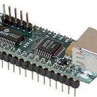
DLP-245SX
Manufacturer Part Number
DLP-245SX
Description
Interface Modules & Development Tools USB/Micro Dev Board
Manufacturer
DLP Design Inc
Datasheet
1.DLP-245SX.pdf
(14 pages)
Specifications of DLP-245SX
Interface Type
USB
Data Bus Width
8 bit
Operating Supply Voltage
5.25 V
Product
Interface Modules
For Use With/related Products
SX28
Lead Free Status / RoHS Status
Lead free / RoHS Compliant


TABLE 1: DLP-245SX PINOUT DESCRIPTION
Pin #
10
11
12
1
2
3
4
5
6
7
8
9
Description
Ground
A0
A1
A2
MCLR*
used.
Ground
RESET#
not used.
RESETO#
2ms after VCC>3.5v and the internal clock starts up, then clamps its output to the 3.3v
output of the internal regulator. Taking RESET# low will also force RESETO# to
go high impedance. RESET0# is NOT affected by a USB Bus Reset.
GROUND
3V3OUT
internal 3.3v supply to the USB transceiver cell and the RSTOUT# pin. A small amount of current
(<=5mA) can be drawn from this pin to power external 3.3v logic if required.
Ground
SWVCC
and Q1 MOSFET power switch. R5 and C3 control the power-up rate to help limit inrush current.
(I/O) Port Pin A0 connected to the SX28 microcontroller
(I/O) Port Pin C2 connected to the SX28 microcontroller.
(I/O) Port Pin C3 connected to the SX28 microcontroller.
(In) Can be used by an external device to reset the SX28. Can be left disconnected if not
(Out) Power from EXTVCC (Pin 19) controlled via Pin 10 (POWERN#) of the FT245BM
(In) Can be used by an external device to reset the FT245BM. Can be left disconnected if
(Out) Output from the integrated L.D.O. regulator. Its primary purpose is to provide the
(Out) Output of the FT245BM’s internal Reset Generator. Stays high impedance for ~
16
1
11
32
17
Related parts for DLP-245SX
Image
Part Number
Description
Manufacturer
Datasheet
Request
R

Part Number:
Description:
Zigbee / 802.15.4 Modules & Development Tools USE 626-DLP-RF2-Z
Manufacturer:
DLP Design Inc
Datasheet:
Part Number:
Description:
Zigbee / 802.15.4 Modules & Development Tools TTL SERIAL INTERFACE MODULE
Manufacturer:
DLP Design Inc
Datasheet:

Part Number:
Description:
MODULE USB-TO-TTL SRL UART CONV
Manufacturer:
DLP Design Inc
Datasheet:

Part Number:
Description:
Interface Modules & Development Tools FLASH2 TARGET BOARD 18F2321 w/IDE 2k Ltd
Manufacturer:
DLP Design Inc

Part Number:
Description:
Interface Modules & Development Tools FLASH2 TARGET BOARD 16F917 w/IDE 2k Ltd
Manufacturer:
DLP Design Inc

Part Number:
Description:
Interface Modules & Development Tools FLASH2 TARGET BOARD 18F4420 w/IDE 2k Ltd
Manufacturer:
DLP Design Inc
Part Number:
Description:
Zigbee / 802.15.4 Modules & Development Tools TTL SERIAL INTERFACE MODULE
Manufacturer:
DLP Design Inc
Datasheet:

Part Number:
Description:
Interface Modules & Development Tools USB FPGA Module w/ Xilinx XC3S400A
Manufacturer:
DLP Design Inc
Datasheet:

Part Number:
Description:
Interface Modules & Development Tools Dual Ch USB Adapter w/ FTDI FT2232H
Manufacturer:
DLP Design Inc
Datasheet:

Part Number:
Description:
MODULE DATA-ACQUISITION 8-CH
Manufacturer:
DLP Design Inc
Datasheet:

Part Number:
Description:
MODULE USB-MCU FT245RL W/16F877A
Manufacturer:
DLP Design Inc
Datasheet:

Part Number:
Description:
MODULE USB-TO-FPGA TRAINING TOOL
Manufacturer:
DLP Design Inc
Datasheet:

Part Number:
Description:
MODULE USB-MCU FT232R W/18F2410
Manufacturer:
DLP Design Inc
Datasheet:

Part Number:
Description:
MODULE USB-MCU FT245RL W/SX48
Manufacturer:
DLP Design Inc
Datasheet:

Part Number:
Description:
MODULE USB-MCU FT2232D W/16F877A
Manufacturer:
DLP Design Inc
Datasheet: