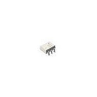
4N39W Fairchild Semiconductor, 4N39W Datasheet - Page 2

4N39W
Manufacturer Part Number
4N39W
Description
Triac & SCR Output Optocouplers Optocoupler Photo SCR Output
Manufacturer
Fairchild Semiconductor
Datasheet
1.4N39W.pdf
(9 pages)
Specifications of 4N39W
Configuration
1
Maximum Continuous Output Current
300 mA
Maximum Input Current
60 mA
Maximum Operating Temperature
+ 100 C
Maximum Power Dissipation
450 mW
Maximum Reverse Diode Voltage
6 V
Maximum Turn-on Time
50 us
Minimum Operating Temperature
- 55 C
Output Type
AC
Package / Case
PDIP-6
Typical Input Voltage
1.1 V
Zero-crossing Circuit
No
Output Device
SCR
Isolation Voltage
5300 Vrms
Peak Output Voltage (vdrm)
200 V
Maximum Input Voltage
1.5 V
Maximum Output Voltage
140 VAC
Minimum Trigger Current
30 mA (Max)
Number Of Elements
1
Forward Voltage
1.5V
Repetitive Peak Off-state Volt
200V
Operating Temp Range
-55C to 100C
Output Current
300mA
Package Type
PDIP
Reverse Breakdown Voltage
6V
Mounting
Through Hole
Pin Count
6
Trigger Current
30mA
Zero Crossing Circuit
No
Operating Temperature Classification
Industrial
Forward Current
60mA
Power Dissipation
450mW
Lead Free Status / RoHS Status
Lead free / RoHS Compliant
Note
** Typical values at T
www.fairchildsemi.com
EMITTER
DETECTOR
Characteristics
Package Capacitance
(input to output)
Coupled dv/dt, input to output
(figure 13)
* Indicates JEDEC Registered Data
*Input Current to Trigger
*Turn-On Time
ELECTRICAL CHARACTERISTICS
INDIVIDUAL COMPONENT CHARACTERISTICS
TRANSFER CHARACTERISTICS
ISOLATION CHARACTERISTICS
Parameter
Input Forward Voltage
Reverse Leakage Current
Capacitance
Peak Off-State Voltage
Peak Reverse Voltage
On-State Voltage
Off-State Current
Reverse Current
Holding Current
Characteristic
*Input-Output Isolation Voltage
*Isolation Resistance
Isolation Capacitance
A
= 25°C
R
V
R
V
V
V
GK
V
Input to Output Voltage = 0
R
AK
V
GK
V
AK
Fx
AK
= 200 V, T
I
DM
F
F
Test Conditions
= 10 k , RL = 200
Test Conditions
= 100 V, R
= 0 mA, R
= 50V, R
= 50 V, R
= 10 k
= 50 V, I
= 0 V, f = 1.0 MHz
= 200 V, T
I
I
T
f = 1 MHz
T
F
V
A
= 300 mA
= 10 mA
R
=100 °C
A
=100 °C, I
= 3 V
GK
GK
F
GK
GK
A
( I
T
= 30 mA
= 100 °C,
= 10 k
A
= 10 k
I-0
= 27 k
= 27 k
=100 °C
(T
F
(T
= 0 mA
A
1 µA, Vrms, t = 1 min.)
A
= 25°C Unless otherwise specified.)
(V
= 25 °C Unless otherwise specified.)
I-O
(V
Test Conditions
=
Symbol
I-O
Symbol
dV/dt
C
V
V
I
t
I
= 500 VDC)
V
C
V
FT
on
DM
I
I
I
I-O
2 OF 8
DM
RM
R
R
H
f = 1 MHz)
F
T
J
PHOTO SCR OPTOCOUPLERS
Device
Device
4N39
4N40
4N39
4N40
4N39
4N40
4N39
4N40
4N39
4N40
ALL
ALL
ALL
All
All
All
All
All
Symbol
V
R
C
ISO
ISO
ISO
5300
Min
500
10
Min
200
400
200
400
Min
11
Typ**
Typ**
Typ**
0.8
1.1
50
4N39
2/27/01
Max
Max
Max
150
150
1.5
1.3
1.0
10
50
50
30
14
50
2
DS300381
Vac(rms)
4N40
Units
Units
V/ S
Unit
mA
mA
µA
pF
µA
µA
pF
!
pf
V
V
V
V
A


