4N39W Fairchild Semiconductor, 4N39W Datasheet
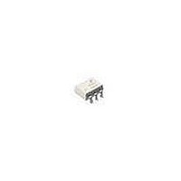
Triac & SCR Output Optocouplers Optocoupler Photo SCR Output

4N39W

Manufacturer Part Number
4N39W
Description
Triac & SCR Output Optocouplers Optocoupler Photo SCR Output
Manufacturer
Fairchild Semiconductor
Datasheet

Specifications of 4N39W

Configuration
1
Maximum Continuous Output Current
300 mA
Maximum Input Current
60 mA
Maximum Operating Temperature
+ 100 C
Maximum Power Dissipation
450 mW
Maximum Reverse Diode Voltage
6 V
Maximum Turn-on Time
50 us
Minimum Operating Temperature
- 55 C
Output Type
AC
Package / Case
PDIP-6
Typical Input Voltage
1.1 V
Zero-crossing Circuit
No
Output Device
SCR
Isolation Voltage
5300 Vrms
Peak Output Voltage (vdrm)
200 V
Maximum Input Voltage
1.5 V
Maximum Output Voltage
140 VAC
Minimum Trigger Current
30 mA (Max)
Number Of Elements
1
Forward Voltage
1.5V
Repetitive Peak Off-state Volt
200V
Operating Temp Range
-55C to 100C
Output Current
300mA
Package Type
PDIP
Reverse Breakdown Voltage
6V
Mounting
Through Hole
Pin Count
6
Trigger Current
30mA
Zero Crossing Circuit
No
Operating Temperature Classification
Industrial
Forward Current
60mA
Power Dissipation
450mW
Lead Free Status / RoHS Status
Lead free / RoHS Compliant
Note
** Typical values at T
DS300381
DESCRIPTION
FEATURES
APPLICATIONS
TOTAL DEVICE
EMITTER
DETECTOR
The 4N39 and 4N40 have a gallium-arsenide infrared
emitting diode optically coupled with a light activated sil-
icon controlled rectifier in a dual in-line package.
• 10 A, T
• 25 W logic indicator lamp driver
• 400 V symmetrical transistor coupler
• Underwriters Laboratory (UL) recognized
• Low power logic circuits
• Telecommunications equipment
• Portable electronics
• Solid state relays
• Interfacing coupling systems of different potentials and impedances.
* Indicates JEDEC Registered Data
Parameter
*Storage Temperature
*Operating Temperature
*Lead Solder Temperature
*Total Device Power Dissipation (-55°C to 50 °C)
*Continuous Forward Current
*Reverse Voltage
*Forward Current - Peak (300 µs, 2% Duty Cycle)
*LED Power Dissipation (-55°C to 50 °C)
*Off-State And Reverse Voltage
*Peak Reverse Gate Voltage
*Direct On-State Current
*Surge On-State Current (100 µs)
*Peak Gate Current
*Detector Power Dissipation (-55°C to 50°C)
2001 Fairchild Semiconductor Corporation
Derate above 50°C
Derate above 50°C
Derate above 50°C
2
L compatible, solid state relay
2/27/01
A
= 25°C
File #E90700
Symbol
I
T
T
T
F
P
V
P
P
OPR
6
STG
SOL
(pk)
6
I
F
D
R
D
D
1 OF 8
PHOTO SCR OPTOCOUPLERS
1
1
Device
4N39
4N40
All
All
All
All
All
All
All
All
All
6
1
260 for 10 sec
-55 to +150
-55 to +100
Value
450
100
200
400
300
400
9.0
1.0
2.0
8.0
60
10
10
6
6
CATHODE
ANODE
www.fairchildsemi.com
N/C
4N39
1
2
3
SCHEMATIC
mW/°C
mW/°C
mW/°C
Units
mW
mW
mW
mA
mA
mA
°C
°C
°C
V
A
V
V
V
A
4N40
6 GATE
5
4
ANODE
CATHODE

Related parts for 4N39W

4N39W Summary of contents

Page 1

... On-State Current *Surge On-State Current (100 µs) *Peak Gate Current *Detector Power Dissipation (-55°C to 50°C) Derate above 50°C Note * Indicates JEDEC Registered Data ** Typical values 25°C A 2001 Fairchild Semiconductor Corporation DS300381 2/27/01 PHOTO SCR OPTOCOUPLERS File #E90700 6 1 Symbol ...

Page 2

ELECTRICAL CHARACTERISTICS INDIVIDUAL COMPONENT CHARACTERISTICS Parameter Test Conditions EMITTER Input Forward Voltage Reverse Leakage Current Capacitance 1.0 MHz F DETECTOR Peak Off-State Voltage Peak Reverse Voltage On-State Voltage V ...

Page 3

Figure 1. Input Current To Trigger vs. Anode-Cathode Voltage NORMALIZED 300 10K .5 27K 56K . ANODE TO CATHODE VOLTAGE (VOLTS) AK Figure 3. Input Current ...

Page 4

Figure 7. Holding Current vs. Temperature 10,000 5,000 R GK 1000 1K 500 10K 100 27K 50 56K -40 - AMBIENT TEMPERATURE ( ˚C) A Figure 9. Off-State Forward Current vs. Temperature ...

Page 5

Vp . Fig. 13 Coupled dv/dt - Test Circuit TYPICAL APPLICATIONS 2 10A COMPATIBLE, SOLID STATE RELAY Use of the 4N40 for high sensi- tivity, 5300 V isolation capability, provides this highly reliable solid +5V state ...

Page 6

Package Dimensions (Through Hole) PIN 1 ID. 0.270 (6.86) 0.240 (6.10) 0.350 (8.89) 0.330 (8.38) 0.070 (1.78) 0.045 (1.14) 0.200 (5.08) 0.135 (3.43) 0.020 (0.51) 0.154 (3.90) MIN 0.100 (2.54) 0.016 (0.40) 0.008 (0.20) 0.022 (0.56) 0° to 15° 0.016 ...

Page 7

ORDERING INFORMATION Option 300 300W 3S 3SD Carrier Tape Specifications (“D” Taping Orientation) 4.85 ± 0.20 13.2 ± 0.2 0.1 MAX NOTE All dimensions are millimeters DS300381 2/27/01 PHOTO SCR OPTOCOUPLERS Order Entry Identifier .S .SD .W ...

Page 8

MARKING INFORMATION Definitions Reflow Profile (Black Package, No Suffix) 300 250 225 C peak 200 150 Time above 183° C, 60–150 sec 100 50 Ramp C/sec 0 0 0.5 1 1.5 ...

Page 9

... TRADEMARKS The following are registered and unregistered trademarks Fairchild Semiconductor owns or is authorized to use and is not intended exhaustive list of all such trademarks.  ACEx™ FAST ActiveArray™ FASTr™ Bottomless™ FPS™ CoolFET™ FRFET™ CROSSVOLT™ GlobalOptoisolator™ ...

Related keywords