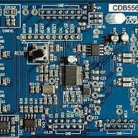
CDB5566 Cirrus Logic Inc, CDB5566 Datasheet - Page 25
CDB5566
Manufacturer Part Number
CDB5566
Description
Dev Bd For I/C 24-bit, Diff, 5kSPS, DAQ
Manufacturer
Cirrus Logic Inc
Type
A/Dr
Specifications of CDB5566
Number Of Adc's
1
Number Of Bits
24
Sampling Rate (per Second)
5k
Data Interface
SPI™
Inputs Per Adc
2 Differential
Input Range
0 ~ 4.096 V
Power (typ) @ Conditions
20mW @ 5kSPS
Voltage Supply Source
Analog and Digital, Dual ±
Operating Temperature
-40°C ~ 85°C
Utilized Ic / Part
CS5566
Conversion Rate
5 KSPS
Resolution
24 bit
Maximum Clock Frequency
8 MHz
Interface Type
SPI
Supply Voltage (max)
3.3 V
Supply Voltage (min)
- 2.5 V
Product
Data Conversion Development Tools
Lead Free Status / RoHS Status
Contains lead / RoHS non-compliant
For Use With/related Products
CS5566
Lead Free Status / RoHS Status
Contains lead / RoHS non-compliant
Other names
598-1557
CDB-5566
CDB-5566


3.12 Power Supplies & Grounding
The CS5566 can be configured to operate with its analog supply operating from 5V, or with its analog sup-
plies operating from ±2.5V. The digital interface supports digital logic operating from either 1.8V, 2.5V, or
3.3V.
Figure 8
illustrates the device configured to operate from 5V analog. Note that the schematic indicates a 47 µF ca-
pacitor between V1+ and V1-. This capacitor is necessary to reduce the peak current required from the
power supply during conversion. See
To maximize converter performance, the analog ground and the logic ground for the converter should be
connected at the converter. In the dual analog supply configuration, the analog ground for the ±2.5V sup-
plies should be connected to the VLR pin at the converter with the converter placed entirely over the an-
alog ground plane.
In the single analog supply configuration (+5V), the ground for the +5V supply should be directly tied to
the VLR pin of the converter with the converter placed entirely over the analog ground plane. Refer to
Figure 9
3.13 Using the CS5566 in Multiplexing Applications
The actual conversion process inside the CS5566 begins 1182 MCLK cycles after the CONV signal is tak-
en low. This would be over 147 microseconds when MCLK = 8 MHz. If the input channel of an external
multiplexer is changed coincident with CONV going low, the 1182 MCLK delay should be more than an
adequate time for settling. If there is an operational amplifier between the multiplexer and the converter,
one should be certain that the amplifier can settle within the 1182 MCLK delay period. If not, the multiplex-
er will need to be switched some time prior to CONV going low.
3.14 Synchronizing Multiple Converters
Many measurement systems have multiple converters that need to operate synchronously. The convert-
ers should all be driven from the same master clock. In this configuration, the converters will convert syn-
chronously if the same CONV signal is used to drive all the converters, and CONV falls on a falling edge
of MCLK. If CONV is held low continuously, reset (RST) can be used to synchronize multiple converters
if RST is released on a falling edge of MCLK.
DS806PP1
on page 18 illustrates the device configured to operate from ±2.5V analog.
on page 19.
Power Consumption
3/25/08
on page 16 for a more detailed discussion.
Figure 9
CS5566
on page 19
25
Related parts for CDB5566
Image
Part Number
Description
Manufacturer
Datasheet
Request
R

Part Number:
Description:
Development Kit
Manufacturer:
Cirrus Logic Inc
Datasheet:
Part Number:
Description:
Development Kit
Manufacturer:
Cirrus Logic Inc
Datasheet:


Part Number:
Description:
High-efficiency PFC + Fluorescent Lamp Driver Reference Design
Manufacturer:
Cirrus Logic Inc
Datasheet:
Part Number:
Description:
Development Kit
Manufacturer:
Cirrus Logic Inc
Datasheet:
Part Number:
Description:
Development Kit
Manufacturer:
Cirrus Logic Inc
Datasheet:

Part Number:
Description:
Development Kit
Manufacturer:
Cirrus Logic Inc
Datasheet:
Part Number:
Description:
Development Kit
Manufacturer:
Cirrus Logic Inc
Datasheet:
Part Number:
Description:
Development Kit
Manufacturer:
Cirrus Logic Inc
Datasheet:
Part Number:
Description:
Development Kit
Manufacturer:
Cirrus Logic Inc
Datasheet:

Part Number:
Description:
EVALUATION BOARD FOR CS8427
Manufacturer:
Cirrus Logic Inc
Datasheet:

Part Number:
Description:
BOARD EVAL FOR CS8416 RCVR
Manufacturer:
Cirrus Logic Inc
Datasheet:

Part Number:
Description:
EVALUATION BOARD FOR CS8420
Manufacturer:
Cirrus Logic Inc
Datasheet:

Part Number:
Description:
KIT DEVELOPMENT EP9315 ARM9
Manufacturer:
Cirrus Logic Inc
Datasheet:

Part Number:
Description:
KIT DEVELOPMENT EP9302 ARM9
Manufacturer:
Cirrus Logic Inc
Datasheet: