CDB5566 Cirrus Logic Inc, CDB5566 Datasheet - Page 16
CDB5566
Manufacturer Part Number
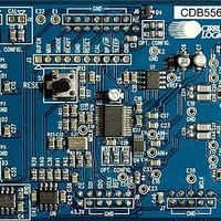
CDB5566
Description
Dev Bd For I/C 24-bit, Diff, 5kSPS, DAQ
Manufacturer
Cirrus Logic Inc
Type
A/Dr
Specifications of CDB5566
Number Of Adc's
1
Number Of Bits
24
Sampling Rate (per Second)
5k
Data Interface
SPI™
Inputs Per Adc
2 Differential
Input Range
0 ~ 4.096 V
Power (typ) @ Conditions
20mW @ 5kSPS
Voltage Supply Source
Analog and Digital, Dual ±
Operating Temperature
-40°C ~ 85°C
Utilized Ic / Part
CS5566
Conversion Rate
5 KSPS
Resolution
24 bit
Maximum Clock Frequency
8 MHz
Interface Type
SPI
Supply Voltage (max)
3.3 V
Supply Voltage (min)
- 2.5 V
Product
Data Conversion Development Tools
Lead Free Status / RoHS Status
Contains lead / RoHS non-compliant
For Use With/related Products
CS5566
Lead Free Status / RoHS Status
Contains lead / RoHS non-compliant
Other names
598-1557
CDB-5566
CDB-5566


3.3 Clock
The CS5566 can be operated from its internal oscillator or from an external master clock. The state of
MCLK determines which clock source will be used. If MCLK is tied low, the internal oscillator will start and
be used as the clock source for the converter. If an external CMOS-compatible clock is input into MCLK
the converter will power down the internal oscillator and use the external clock. If the MCLK pin is held
high, the internal oscillator will be held in the stopped state. The MCLK input can be held high to delete
clock cycles to aid in operating multiple converters in different phase relationships.
The internal oscillator can be used if the signals to be measured are essentially DC. The internal oscillator
exhibits jitter at about 500 picoseconds rms. If the CS5566 is used to digitize AC signals, an external
low-jitter clock source should be used.
If the internal oscillator is used as the clock for the CS5566, the maximum conversion rate will be dictated
by the oscillator frequency.
If driven from an external MCLK source, the fast rise and fall times of the MCLK signal can result in clock
coupling from the internal bond wire of the IC to the analog input. Adding a 50 ohm resistor on the external
MCLK source significantly reduces this effect.
3.4 Voltage Reference
The voltage reference for the CS5566 can range from 2.4 volts to 4.2 volts. A 4.096 volt reference is re-
quired to achieve the specified performance.
reference with either a single +5 V analog supply or with ±2.5 V.
For optimum performance, the voltage reference device should be one that provides a capacitor connec-
tion to provide a means of noise filtering, or the output should include some type of bandwidth-limiting fil-
ter. Some 4.096 volt reference devices need only 5 volts total supply for operation and can be connected
as shown in
output capacitor.
Some older 4.096 voltage reference designs require more headroom and must operate from an input volt-
age of 5.5 to 6.5 volts. If this type of voltage reference is used ensure that when power is applied to the
system, the voltage reference rise time is slower than the rise time of the V1+ and V1- power supply volt-
age to the converter. An example circuit to slow the output startup time of the reference is illustrated in
Figure
16
7.
Figure 8
or
5.5 to 15 V
Figure
10µF
2k
9. The reference should have a local bypass capacitor and an appropriate
Figure 7. Voltage Reference Circuit
GND
VIN
VOUT
Figure 8
3/25/08
4.096 V
Refer to V1- and VREF1 pins.
and
Figure 9
illustrate the connection of the voltage
CS5566
DS806PP1
Related parts for CDB5566
Image
Part Number
Description
Manufacturer
Datasheet
Request
R

Part Number:
Description:
Development Kit
Manufacturer:
Cirrus Logic Inc
Datasheet:
Part Number:
Description:
Development Kit
Manufacturer:
Cirrus Logic Inc
Datasheet:


Part Number:
Description:
High-efficiency PFC + Fluorescent Lamp Driver Reference Design
Manufacturer:
Cirrus Logic Inc
Datasheet:
Part Number:
Description:
Development Kit
Manufacturer:
Cirrus Logic Inc
Datasheet:
Part Number:
Description:
Development Kit
Manufacturer:
Cirrus Logic Inc
Datasheet:

Part Number:
Description:
Development Kit
Manufacturer:
Cirrus Logic Inc
Datasheet:
Part Number:
Description:
Development Kit
Manufacturer:
Cirrus Logic Inc
Datasheet:
Part Number:
Description:
Development Kit
Manufacturer:
Cirrus Logic Inc
Datasheet:
Part Number:
Description:
Development Kit
Manufacturer:
Cirrus Logic Inc
Datasheet:

Part Number:
Description:
EVALUATION BOARD FOR CS8427
Manufacturer:
Cirrus Logic Inc
Datasheet:

Part Number:
Description:
BOARD EVAL FOR CS8416 RCVR
Manufacturer:
Cirrus Logic Inc
Datasheet:

Part Number:
Description:
EVALUATION BOARD FOR CS8420
Manufacturer:
Cirrus Logic Inc
Datasheet:

Part Number:
Description:
KIT DEVELOPMENT EP9315 ARM9
Manufacturer:
Cirrus Logic Inc
Datasheet:

Part Number:
Description:
KIT DEVELOPMENT EP9302 ARM9
Manufacturer:
Cirrus Logic Inc
Datasheet: