CDB5566 Cirrus Logic Inc, CDB5566 Datasheet - Page 17
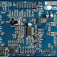
CDB5566
Manufacturer Part Number
CDB5566
Description
Dev Bd For I/C 24-bit, Diff, 5kSPS, DAQ
Manufacturer
Cirrus Logic Inc
Type
A/Dr
Specifications of CDB5566
Number Of Adc's
1
Number Of Bits
24
Sampling Rate (per Second)
5k
Data Interface
SPI™
Inputs Per Adc
2 Differential
Input Range
0 ~ 4.096 V
Power (typ) @ Conditions
20mW @ 5kSPS
Voltage Supply Source
Analog and Digital, Dual ±
Operating Temperature
-40°C ~ 85°C
Utilized Ic / Part
CS5566
Conversion Rate
5 KSPS
Resolution
24 bit
Maximum Clock Frequency
8 MHz
Interface Type
SPI
Supply Voltage (max)
3.3 V
Supply Voltage (min)
- 2.5 V
Product
Data Conversion Development Tools
Lead Free Status / RoHS Status
Contains lead / RoHS non-compliant
For Use With/related Products
CS5566
Lead Free Status / RoHS Status
Contains lead / RoHS non-compliant
Other names
598-1557
CDB-5566
CDB-5566


3.5 Analog Input
The analog input of the converter is fully differential with a peak-to-peak input of 4.096 volts on each input.
Therefore, the differential, peak-to-peak input is 8.192 volts. This is illustrated in
These diagrams also illustrate a differential buffer amplifier configuration for driving the CS5566.
The capacitors at the outputs of the amplifiers provide a charge reservoir for the dynamic current from the
A/D inputs while the resistors isolate the dynamic current from the amplifier. The amplifiers can be pow-
ered from higher supplies than those used by the A/D but precautions should be taken to ensure that the
opamp output voltage remains within the power supply limits of the A/D, especially under start-up condi-
tions.
3.6 Output Coding Format
The reference voltage directly defines the input voltage range in both the unipolar and bipolar configura-
tions. In the unipolar configuration (BP/UP low), the first code transition occurs 0.5 LSB above zero, and
the final code transition occurs 1.5 LSBs below VREF. In the bipolar configuration (BP/UP high), the first
code transition occurs 0.5 LSB above -VREF and the last transition occurs 1.5 LSBs below +VREF. See
Table 1
DS806PP1
NOTE: VREF = (VREF+) - (VREF-)
NOTE: VREF = (VREF+) - (VREF-)
for the output coding of the converter.
Table 1. Output Coding, Two’s Complement
Unipolar Input Voltage
Bipolar Input Voltage
Table 2. Output Coding, Offset Binary
<(-VREF+0.5 LSB)
(VREF/2)-0.5 LSB
>(VREF-1.5 LSB)
>(VREF-1.5 LSB)
-VREF+0.5 LSB
VREF-1.5 LSB
VREF-1.5 LSB
<(+0.5 LSB)
+0.5 LSB
-0.5 LSB
3/25/08
Complement
7F FF FF
7F FF FE
FF FF FF
FF FF FF
FF FF FF
FF FF FE
7F FF FF
7F FF FF
00 00 00
80 00 01
80 00 00
80 00 00
80 00 00
00 00 01
00 00 00
00 00 00
Binary
Offset
Two’s
Figure 8
and
CS5566
Figure
17
9.
Related parts for CDB5566
Image
Part Number
Description
Manufacturer
Datasheet
Request
R

Part Number:
Description:
Development Kit
Manufacturer:
Cirrus Logic Inc
Datasheet:
Part Number:
Description:
Development Kit
Manufacturer:
Cirrus Logic Inc
Datasheet:


Part Number:
Description:
High-efficiency PFC + Fluorescent Lamp Driver Reference Design
Manufacturer:
Cirrus Logic Inc
Datasheet:
Part Number:
Description:
Development Kit
Manufacturer:
Cirrus Logic Inc
Datasheet:
Part Number:
Description:
Development Kit
Manufacturer:
Cirrus Logic Inc
Datasheet:

Part Number:
Description:
Development Kit
Manufacturer:
Cirrus Logic Inc
Datasheet:
Part Number:
Description:
Development Kit
Manufacturer:
Cirrus Logic Inc
Datasheet:
Part Number:
Description:
Development Kit
Manufacturer:
Cirrus Logic Inc
Datasheet:
Part Number:
Description:
Development Kit
Manufacturer:
Cirrus Logic Inc
Datasheet:

Part Number:
Description:
EVALUATION BOARD FOR CS8427
Manufacturer:
Cirrus Logic Inc
Datasheet:

Part Number:
Description:
BOARD EVAL FOR CS8416 RCVR
Manufacturer:
Cirrus Logic Inc
Datasheet:

Part Number:
Description:
EVALUATION BOARD FOR CS8420
Manufacturer:
Cirrus Logic Inc
Datasheet:

Part Number:
Description:
KIT DEVELOPMENT EP9315 ARM9
Manufacturer:
Cirrus Logic Inc
Datasheet:

Part Number:
Description:
KIT DEVELOPMENT EP9302 ARM9
Manufacturer:
Cirrus Logic Inc
Datasheet: