AD9913/PCBZ Analog Devices Inc, AD9913/PCBZ Datasheet - Page 6
AD9913/PCBZ
Manufacturer Part Number
AD9913/PCBZ
Description
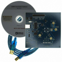
Eval Board
Manufacturer
Analog Devices Inc
Series
AgileRF™r
Datasheet
1.AD9913BCPZ.pdf
(32 pages)
Specifications of AD9913/PCBZ
Silicon Manufacturer
Analog Devices
Application Sub Type
Direct Digital Synthesizer
Kit Application Type
Clock & Timing
Silicon Core Number
AD9913
Kit Contents
Board
Tool / Board Applications
D/A Converter
Main Purpose
Timing, Direct Digital Synthesis (DDS)
Embedded
No
Utilized Ic / Part
AD9913
Primary Attributes
10-Bit DAC, 32-Bit Tuning Word Width
Secondary Attributes
250MHz, Graphical User Interface
Lead Free Status / RoHS Status
Lead free / RoHS Compliant


AD9913
PIN CONFIGURATION AND FUNCTION DESCRIPTIONS
Table 3. Pin Function Descriptions
Pin No.
1
2
3
4
5
6
7
8
9
10
11, 15,
18, 21,
23
12, 16,
17, 22
13
14
19
20
24
25
Mnemonic
PS2/ADR5/D5
PS1/ADR4/D4
PS0/ADR3/D3
DVDD
DGND
ADR2/D2
ADR1/D1
ADR0/D0
SYNC_CLK
SER/PAR
AGND
AVDD
REF_CLK
REF_CLK
IOUT
IOUT
RSET
MASTER_RESET
I/O
I/O
I/O
I/O
I
I
I/O
I/O
I/O
O
I
I
I
I
I
O
O
I
I
Description
Multipurpose pin: Profile Select Pin (PS2) in Direct Switch Mode, Parallel Port Address Line (ADR5), and
Data Line (D5) to program registers.
Multipurpose pin: Profile Select Pin (PS1) in Direct Switch Mode or Linear Sweeping Mode, Parallel Port
Address Line (ADR4), and Data Line (D4) to program registers.
Multipurpose pin: Profile Select Pin (PS0) in Direct Switch Mode or Linear Sweeping Mode, Parallel Port
Address Line (ADR3), and Data Line (D3) to program registers.
Digital Power Supply (1.8 V).
Digital Ground.
Parallel Port Address Line 2 and Data Line 2.
Parallel Port Address Line 1and Data Line 1.
Parallel Port Address Line 0 and Data Line 0.
Clock Out. The profile pins [PS0:PS2] and the IO_UPDATE pin (Pin 27) should be set up to the rising
edge of this signal to maintain constant pipe line delay through the device.
Serial Port and Parallel Port Selection. Logic low = serial mode; logic high = parallel mode.
Analog Ground.
Analog Power Supply (1.8 V).
Reference Clock Input. See the REF_CLK Overview section for more details.
Complementary Reference Clock Input. See the REF_CLK Overview section for more details.
Open Source DAC Complementary Output Source. Current mode. Connect through 50 Ω to AGND.
Open Source DAC Output Source. Current mode. Connect through 50 Ω to AGND.
Analog Reference. This pin programs the DAC output full-scale reference current. Attach a 4.64 kΩ
resistor to AGND.
Master Reset, Digital Input (Active High). This pin clears all memory elements and reprograms registers
to default values.
PS2/ADR5/D5
PS1/ADR4/D4
PS0/ADR3/D3
NOTES
1. EXPOSED PAD SHOULD BE SOLDERED TO GROUND.
ADR2/D2
ADR1/D1
ADR0/D0
DGND
DVDD
Figure 3. Pin Configuration
1
2
3
4
5
6
7
8
Rev. A | Page 6 of 32
(Not to Scale)
PIN 1
INDICATOR
AD9913
TOP VIEW
24 RSET
23 AGND
22 AVDD
21 AGND
20 IOUT
19 IOUT
18 AGND
17 AVDD
Related parts for AD9913/PCBZ
Image
Part Number
Description
Manufacturer
Datasheet
Request
R


Part Number:
Description:
±1.7g Dual-Axis IMEMS Accelerometer Evaluation Board
Manufacturer:
Analog Devices Inc
Datasheet:

Part Number:
Description:
Inertial Sensor Evaluation System
Manufacturer:
Analog Devices Inc
Datasheet:
Part Number:
Description:
Manufacturer:
Analog Devices Inc
Datasheet:
Part Number:
Description:
Manufacturer:
Analog Devices Inc
Datasheet:
Part Number:
Description:
Manufacturer:
Analog Devices Inc
Datasheet:
Part Number:
Description:
Manufacturer:
Analog Devices Inc
Datasheet:
Part Number:
Description:
Manufacturer:
Analog Devices Inc
Datasheet:
Part Number:
Description:
Manufacturer:
Analog Devices Inc
Datasheet:
Part Number:
Description:
Manufacturer:
Analog Devices Inc
Datasheet:
Part Number:
Description:
Manufacturer:
Analog Devices Inc
Datasheet:
Part Number:
Description:
Manufacturer:
Analog Devices Inc
Datasheet:
Part Number:
Description:
Manufacturer:
Analog Devices Inc
Datasheet: