AD9913/PCBZ Analog Devices Inc, AD9913/PCBZ Datasheet - Page 12
AD9913/PCBZ
Manufacturer Part Number
AD9913/PCBZ
Description
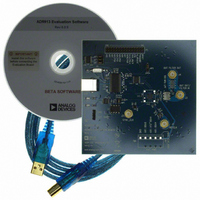
Eval Board
Manufacturer
Analog Devices Inc
Series
AgileRF™r
Datasheet
1.AD9913BCPZ.pdf
(32 pages)
Specifications of AD9913/PCBZ
Silicon Manufacturer
Analog Devices
Application Sub Type
Direct Digital Synthesizer
Kit Application Type
Clock & Timing
Silicon Core Number
AD9913
Kit Contents
Board
Tool / Board Applications
D/A Converter
Main Purpose
Timing, Direct Digital Synthesis (DDS)
Embedded
No
Utilized Ic / Part
AD9913
Primary Attributes
10-Bit DAC, 32-Bit Tuning Word Width
Secondary Attributes
250MHz, Graphical User Interface
Lead Free Status / RoHS Status
Lead free / RoHS Compliant


AD9913
THEORY OF OPERATION
DDS CORE
The DDS block generates a reference signal (sine or cosine
based on the selected DDS sine output bit). The parameters of
the reference signal (frequency and phase), are applied to the
DDS at its frequency and phase offset control inputs, as shown
in Figure 19.
The output frequency (f
frequency tuning word (FTW) at the frequency control input to
the DDS. In all modes except for programmable modulus, the
relationship between f
where FTW is a 32-bit integer ranging in value from 0 to
2,147,483,647 (2
full 32-bit range. This range constitutes frequencies from dc to
Nyquist (that is, ½ f
FREQUENCY
CONTROL
CONTROL
OFFSET
DDS SIGNAL CONTROL PARAMETERS
PHASE
f
OUT
=
14
32
⎛
⎜
⎝
FTW
2
SYSTEM
CLOCK
32
31
ACCUMULATOR
− 1), which represents the lower half of the
Figure 19. DDS Block Diagram
SYSCLK
⎞
⎟
⎠
32
32
32-BIT
f
OUT
SYSCLK
OUT
D Q
).
MSB ALIGNED
, FTW, and f
R
ACCUMULATOR
RESET
) of the AD9913 is controlled by the
ACCUMULATOR
CLOCK PORT
32
32
AUXILIARY
15
MSBs
SYSCLK
15
CONVERSION
is:
MULTIPLIER
AMPLITUDE
(SINE OR
COSINE)
32
32
ANGLE
32
PLL
TO
FTW
EXTERNAL
0
1
2
ACCUMULATOR
REGISTER MAP AND TIMING CONTROL
Figure 20. Detailed Block Diagram
+
10
TO DAC
INTERNAL
PHASE
0
1
SELECTION
Z
CLOCK
Rev. A | Page 12 of 32
–1
(1)
SELECTIONS
PROFILE
32
0
1
DDS CORE
14
OFFSET
14
PHASE
The FTW required to generate a desired value of f
by solving Equation 1 for FTW as given in Equation 2
where the round(x) function rounds the argument (the value of
x) to the nearest integer. This is required because the FTW is
constrained to be an integer value.
For applications where rounding to the nearest available fre-
quency is not acceptable, programmable modulus mode enables
additional options.
The relative phase of the DDS signal can be digitally controlled
by means of a 14-bit phase offset word (POW). The phase offset
is applied prior to the angle-to-amplitude conversion block
internal to the DDS core. The relative phase offset (Δθ) is given by
where the upper quantity is for the phase offset expressed as
radian units and the lower quantity as degrees. To find the
POW value necessary to develop an arbitrary Δθ, solve the
above equation for POW and round the result (in a manner
similar to that described for finding an arbitrary FTW in
Equation 1 and Equation 2).
POW
Δ
FTW
I/O PORT
θ
AMPLITUDE
ANGLE TO
=
2
360
=
⎛ π
round
⎜
⎝
⎛
⎜
⎝
POW
POW
2
14
2
14
⎛
⎜
⎜
⎝
10
2
⎞
⎟
⎠
32
⎞
⎟
⎠
DAC
⎛
⎜
⎜
⎝
f
SYSCLK
f
OUT
⎞
⎟
⎟
⎠
⎞
⎟
⎟
⎠
IOUT
IOUT
RSET
OUT
is found
(2)
Related parts for AD9913/PCBZ
Image
Part Number
Description
Manufacturer
Datasheet
Request
R


Part Number:
Description:
±1.7g Dual-Axis IMEMS Accelerometer Evaluation Board
Manufacturer:
Analog Devices Inc
Datasheet:

Part Number:
Description:
Inertial Sensor Evaluation System
Manufacturer:
Analog Devices Inc
Datasheet:
Part Number:
Description:
Manufacturer:
Analog Devices Inc
Datasheet:
Part Number:
Description:
Manufacturer:
Analog Devices Inc
Datasheet:
Part Number:
Description:
Manufacturer:
Analog Devices Inc
Datasheet:
Part Number:
Description:
Manufacturer:
Analog Devices Inc
Datasheet:
Part Number:
Description:
Manufacturer:
Analog Devices Inc
Datasheet:
Part Number:
Description:
Manufacturer:
Analog Devices Inc
Datasheet:
Part Number:
Description:
Manufacturer:
Analog Devices Inc
Datasheet:
Part Number:
Description:
Manufacturer:
Analog Devices Inc
Datasheet:
Part Number:
Description:
Manufacturer:
Analog Devices Inc
Datasheet:
Part Number:
Description:
Manufacturer:
Analog Devices Inc
Datasheet: