AD9913/PCBZ Analog Devices Inc, AD9913/PCBZ Datasheet - Page 4
AD9913/PCBZ
Manufacturer Part Number
AD9913/PCBZ
Description
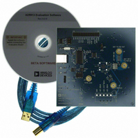
Eval Board
Manufacturer
Analog Devices Inc
Series
AgileRF™r
Datasheet
1.AD9913BCPZ.pdf
(32 pages)
Specifications of AD9913/PCBZ
Silicon Manufacturer
Analog Devices
Application Sub Type
Direct Digital Synthesizer
Kit Application Type
Clock & Timing
Silicon Core Number
AD9913
Kit Contents
Board
Tool / Board Applications
D/A Converter
Main Purpose
Timing, Direct Digital Synthesis (DDS)
Embedded
No
Utilized Ic / Part
AD9913
Primary Attributes
10-Bit DAC, 32-Bit Tuning Word Width
Secondary Attributes
250MHz, Graphical User Interface
Lead Free Status / RoHS Status
Lead free / RoHS Compliant


AD9913
Parameter
MISCELLANEOUS TIMING CHARACTERISTICS
DATA LATENCY (PIPELINE DELAY)
CMOS LOGIC INPUTS
CMOS LOGIC OUTPUTS
POWER SUPPLY CURRENT
POWER CONSUMPTION
1
2
Refer to the Power-Down Features section.
SYSCLK cycle refers to the actual clock frequency used on-chip by the DDS. If the reference clock multiplier is used to multiply the external reference clock frequency,
the SYSCLK frequency is the external frequency multiplied by the reference clock multiplication factor. If the reference clock multiplier and divider are not used, the
SYSCLK frequency is the same as the external reference clock frequency.
Wake-Up Time
Reset Pulse Width High
Modulus Mode
Linear Sweep Mode
Power-Down
PLL Modes
Frequency, Phase-to-DAC Output
Frequency-to-DAC Output
Phase-to-DAC Output
Delta Tuning Word-to-DAC Output (Linear Sweep)
Logic 1 Voltage
Logic 0 Voltage
Logic 1 Current
Logic 0 Current
Input Capacitance
Logic 1 Voltage
Logic 0 Voltage
DVDD (1.8 V) Pin Current Consumption
DAC_CLK_AVDD (1.8 V)
DAC_AVDD (1.8 V) Pin Current Consumption
PLL_AVDD (1.8 V)
CLK_AVDD (1.8 V) Pin Current Consumption
Single Tone Mode
Fast Recovery Mode
Full Sleep Mode
Full
Safe
VCO 1
VCO 2
Differential Input Mode
CMOS Input Mode
Crystal Mode
Differential Input Mode
CMOS Input Mode
Crystal Mode
1
Conditions/Comments
Matched latency enabled
Matched latency disabled
Matched latency disabled
1 mA load
PLL enabled, CMOS input
PLL disabled, differential input
PLL enabled, XTAL input
PLL disabled
PLL disabled
PLL enabled
Rev. A | Page 4 of 32
Min
5
1.2
−700
−700
1.5
Typ
11
11
10
14
3
50
57
52
Max
1
60
0.4
+700
+700
0.125
46.5
4.7
6.2
1.8
4.3
66.5
70.5
68.5
94.6
98.4
15
44.8
11
7.5
5.4
15
11.5
9.4
Unit
SYSCLK cycles
μs
SYSCLK cycles
SYSCLK cycles
SYSCLK cycles
SYSCLK cycles
V
V
nA
nA
pF
V
V
mA
mA
mA
mA
mA
mW
mW
mW
mW
mW
mW
mW
mW
mW
mW
mW
mW
SYSCLK cycles
mW
2
Related parts for AD9913/PCBZ
Image
Part Number
Description
Manufacturer
Datasheet
Request
R


Part Number:
Description:
±1.7g Dual-Axis IMEMS Accelerometer Evaluation Board
Manufacturer:
Analog Devices Inc
Datasheet:

Part Number:
Description:
Inertial Sensor Evaluation System
Manufacturer:
Analog Devices Inc
Datasheet:
Part Number:
Description:
Manufacturer:
Analog Devices Inc
Datasheet:
Part Number:
Description:
Manufacturer:
Analog Devices Inc
Datasheet:
Part Number:
Description:
Manufacturer:
Analog Devices Inc
Datasheet:
Part Number:
Description:
Manufacturer:
Analog Devices Inc
Datasheet:
Part Number:
Description:
Manufacturer:
Analog Devices Inc
Datasheet:
Part Number:
Description:
Manufacturer:
Analog Devices Inc
Datasheet:
Part Number:
Description:
Manufacturer:
Analog Devices Inc
Datasheet:
Part Number:
Description:
Manufacturer:
Analog Devices Inc
Datasheet:
Part Number:
Description:
Manufacturer:
Analog Devices Inc
Datasheet:
Part Number:
Description:
Manufacturer:
Analog Devices Inc
Datasheet: