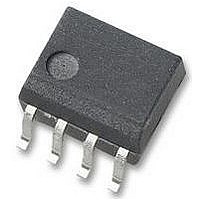
FOD2741BSD Fairchild Semiconductor, FOD2741BSD Datasheet

FOD2741BSD
Specifications of FOD2741BSD
Available stocks
Related parts for FOD2741BSD
FOD2741BSD Summary of contents
Page 1
... GND 6 COMP LED * The compensation network must be attached between pins 6 and 7. © 2003 Fairchild Semiconductor Corporation FOD2741B Pin function description Not connected Phototransistor Collector Phototransistor Emitter Not connected Ground Error Amplifier Compensation. This pin is the output of the error amplifier. * Voltage Feedback. This pin is the inverting input to the error amplifi ...
Page 2
... Derate linearly from 25° rate of 1.42 mW/ °C. 3. Derate linearly from 25° rate of 2.42 mW/ °C. 4. Functional operation under these conditions is not implied. Permanent damage may occur if the device is subjected to conditions outside these ratings. © 2003 Fairchild Semiconductor Corporation OPTICALLY ISOLATED FOD2741B FOD2741 ...
Page 3
... A 2. The dynamic impedance is defined as |Z Figure 2), the total dynamic impedance of the circuit is given by: ∆V R1 ≈ × ------- - ------- - ∆I OUT, TOT OUT R2 © 2003 Fairchild Semiconductor Corporation FOD2741B (T = 25°C Unless otherwise specified.) A Test Conditions ( mA (fig.1) LED COMP mA LED COMP ...
Page 4
... Vcm, to assure that the output will remain high. Common mode transient immunity at output low is the maximum tolerable (negative) dVcm/dt on the trailing edge of the common pulse signal,Vcm, to assure that the output will remain low. © 2003 Fairchild Semiconductor Corporation FOD2741B (T = 25° ...
Page 5
... REF 5 FIG (min) TEST CIRCUIT REF F, LED I (LED REF FIG TEST CIRCUIT REF FIG TEST CIRCUIT CEO © 2003 Fairchild Semiconductor Corporation FOD2741B FIG. 2. ∆ (LED) I CEO Page OPTICALLY ISOLATED ERROR AMPLIFIER FOD2741C I (LED COMP R2 V REF 5 ∆V TEST CIRCUIT REF/ ...
Page 6
... FOD2741A OUT 2.2kΩ V OUT © 2003 Fairchild Semiconductor Corporation FOD2741B 0 Fig. 7 Frequency Response Test Circuit VCM _ + 10V P-P Fig. 8 CMH and CML Test Circuit Page OPTICALLY ISOLATED ERROR AMPLIFIER FOD2741C 47Ω 1µ 0.47V = 12/9/04 ...
Page 7
... T - Ambient Temperature (°C) A Fig. 12 – Off-State Current vs. Ambient Temperature 100 V = 37V -40 - Ambient Temperature (°C) A © 2003 Fairchild Semiconductor Corporation FOD2741B 1.0 0.5 0.0 -0.5 -1 1.30 1.25 1.20 1.15 1.10 1. 100 100 Page OPTICALLY ISOLATED ERROR AMPLIFIER FOD2741C Fig. 9b – ...
Page 8
... I - Forward Current (mA) LED Fig. 18 – Collector Current vs. Collector Voltage 25° VCE - Collector-Emitter Voltage (V) © 2003 Fairchild Semiconductor Corporation FOD2741B 100 0.26 0.24 0.22 0.20 0.18 0.16 0.14 0.12 0. -0.32 -0. 20mA LED -0.36 -0.38 -0. 10mA LED -0 ...
Page 9
... FOD2741A © 2003 Fairchild Semiconductor Corporation FOD2741B Fig. 20 – Voltage Gain vs. Frequency VCC=10V IF=10mA 500Ω 1kΩ -10 -15 0 100 Frequency - kHz Page OPTICALLY ISOLATED ERROR AMPLIFIER FOD2741C RL = 100Ω 1000 12/9/04 ...
Page 10
... OUT > ---------------------------- - 1040µA R TOP © 2003 Fairchild Semiconductor Corporation OPTICALLY ISOLATED ERROR AMPLIFIER FOD2741B Compensation The compensation pin of the FOD2741 provides the opportu- nity for the designer to design the frequency response of the converter. A compensation network may be placed between the COMP pin and the FB pin. In typical low-bandwidth systems, a 0.1µ ...
Page 11
... TYP NOTE All dimensions are in inches (millimeters) © 2003 Fairchild Semiconductor Corporation OPTICALLY ISOLATED FOD2741B Package Dimensions (Surface Mount) 0.390 (9.91) 0.370 (9.40 15° MAX ...
Page 12
... VDE mark (Note: Only appears on parts ordered with VDE 3 option – See order entry table) 4 Two digit year code, e.g., ‘03’ 5 Two digit work week ranging from ‘01’ to ‘53’ 6 Assembly package code © 2003 Fairchild Semiconductor Corporation FOD2741B VDE tested 2741A V XX ...
Page 13
... Tape Width Tape Thickness Sprocket Hole Pitch Sprocket Hole Diameter Sprocket Hole Location Pocket Location Pocket Pitch Pocket Dimensions Cover Tape Width Cover Tape Thickness Max. Component Rotation or Tilt Min. Bending Radius © 2003 Fairchild Semiconductor Corporation FOD2741B User Direction of Feed Symbol ...
Page 14
... FOD2741A Reflow Profile © 2003 Fairchild Semiconductor Corporation FOD2741B 245 C, 10–30 s 300 260 C peak 250 200 150 Time above 183 C, <160 sec 100 50 Ramp up = 2–10 C/sec 0 0 0.5 1 1.5 2 2.5 3 Time (Minute) • Peak reflow temperature: 260 C (package surface temperature) • ...
Page 15
... NEITHER DOES IT CONVEY ANY LICENSE UNDER ITS PATENT RIGHTS, NOR THE RIGHTS OF OTHERS. LIFE SUPPORT POLICY FAIRCHILD’S PRODUCTS ARE NOT AUTHORIZED FOR USE AS CRITICAL COMPONENTS IN LIFE SUPPORT DEVICES OR SYSTEMS WITHOUT THE EXPRESS WRITTEN APPROVAL OF THE PRESIDENT OF FAIRCHILD SEMICONDUCTOR CORPORATION. As used herein: 1. Life support devices or systems are devices or systems ...


