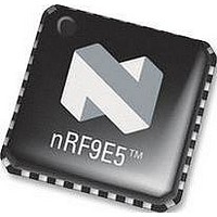
NRF9E5 NORDIC SEMICONDUCTOR, NRF9E5 Datasheet - Page 91

NRF9E5
Manufacturer Part Number
NRF9E5
Description
TRX, 430-928MHZ, MCU/ADC/PWM, SMD
Manufacturer
NORDIC SEMICONDUCTOR
Datasheet
1.NRF9E5.pdf
(108 pages)
Specifications of NRF9E5
Receiving Current
12.5mA
Transmitting Current
30mA
Data Rate
50Kbps
Frequency Range
430MHz To 928MHz
Modulation Type
GFSK
Rf Ic Case Style
QFN
No. Of Pins
32
Supply Voltage Range
1.9V To
Lead Free Status / RoHS Status
Lead free / RoHS Compliant
Available stocks
Company
Part Number
Manufacturer
Quantity
Price
Company:
Part Number:
NRF9E5C
Manufacturer:
NORDIC
Quantity:
5 000
Part Number:
NRF9E5C
Manufacturer:
NORDIC
Quantity:
20 000
PRODUCT SPECIFICATION
nRF9E5 Single Chip Transceiver with Embedded Microcontroller and ADC
18.9.3.2 Mode 2 Receive
Figure 31 illustrates the mode 2 receive timing. Reception begins at the falling edge of a
start bit received on RXD, when enabled by the REN bit. For this purpose, RXD is
sampled sixteen times per bit for any baud rate. When a falling edge of a start bit is
detected, the divide-by-16 counter used to generate the receive clock is reset to align the
counter rollover to the bit boundaries.
For noise rejection, the serial port establishes the content of each received bit by a
majority decision of three consecutive samples in the middle of each bit time. This is
especially true for the start bit. If the falling edge on RXD is not verified by a majority
decision of three consecutive samples (low), then the serial port stops reception and
waits for another falling edge on RXD.
At the middle of the stop bit time, the serial port checks for the following conditions:
If the above conditions are met, the serial port then writes the received byte to the SBUF
register, loads the 9th received bit into RB8, and sets the RI bit. If the above conditions
are not met, the received data is lost, the SBUF register and RB8 bit are not loaded, and
the RI bit is not set. After the middle of the stop bit time, the serial port waits for another
high-to-low transition on the RXD.
18.9.4 Mode 3
Mode 3 provides asynchronous, full-duplex communication, using a total of eleven bits:
The mode 3 transmit and receive operations are identical to mode 2. The mode 3 baud
rate generation is identical to mode 1. That is, mode 3 is a combination of mode 2
protocol and mode 1 baud rate. Figure 32 illustrates the mode 3 transmit timing. Mode 3
operation is identical to that of the standard 8051 when Timers 1 and 2 use CPU_clk/12
(the default).
Main office: Nordic Semiconductor ASA - Vestre Rosten 81, N-7075 Tiller, Norway -Phone +4772898900 - Fax +4772898989
Revision: 1.3
Bit detector
- RI = 0
- If SM2 = 1, the state of the stop bit is 1
- One start bit
- Eight data bits
- One programmable 9th bit
- One stop bit; the data bits are transmitted and received LSB first
sampling
(if SM2 = 0, the state of the stop bit does not matter)
RX CLK
SHIFT
RXD
TXD
RI
TI
START
Figure 31 Serial port Mode 2 Receive Timing.
D0
D1
Page 91 of 108
D2
D3
D4
D5
D6
D7
RB8
STOP
June 2006


