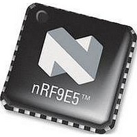
NRF9E5 NORDIC SEMICONDUCTOR, NRF9E5 Datasheet - Page 16

NRF9E5
Manufacturer Part Number
NRF9E5
Description
TRX, 430-928MHZ, MCU/ADC/PWM, SMD
Manufacturer
NORDIC SEMICONDUCTOR
Datasheet
1.NRF9E5.pdf
(108 pages)
Specifications of NRF9E5
Receiving Current
12.5mA
Transmitting Current
30mA
Data Rate
50Kbps
Frequency Range
430MHz To 928MHz
Modulation Type
GFSK
Rf Ic Case Style
QFN
No. Of Pins
32
Supply Voltage Range
1.9V To
Lead Free Status / RoHS Status
Lead free / RoHS Compliant
Available stocks
Company
Part Number
Manufacturer
Quantity
Price
Company:
Part Number:
NRF9E5C
Manufacturer:
NORDIC
Quantity:
5 000
Part Number:
NRF9E5C
Manufacturer:
NORDIC
Quantity:
20 000
PRODUCT SPECIFICATION
nRF9E5 Single Chip Transceiver with Embedded Microcontroller and ADC
Port 0 is controlled by SFR-registers 0x80, 0x93, 0x94 and 0x95 listed in the table
below.
6.2.1 High Current Drive Capability
Odd numbered bits will source high current when the corresponding bit in P0_DRV is
set, where as even number bits will sink high current when the corresponding bit in
P0_DRV is set.
6.3
The P1 port consists of 4 pins, one of which is a hardwired input. The primary function
of the P1 port (when SPI_CTRL is 01) is a SPI master port. The pin EECSN is used as a
chip select for the boot EEPROM, the GPIO bits in port P0 may be used as chip select(s)
for other SPI devices.
P1_ALT.0 can be set to use SCK (P1.0) as a timer 2 control. In that case the CPU
samples this signal every 4 CPU clock periods. MOSI (P1.1) is now a GPIO. When
P0_ALT.0 is 0, also SCK (P1.0) is a GPIO.
MISO (P1.2) is always an input. That is P1_DIR.2 and P1_ALT.2 are ignored.
EECSN (P1.3) is always a GPIO. It will be activated by the default boot loader after
reset and should be connected to the CSN of the boot flash.
Main office: Nordic Semiconductor ASA - Vestre Rosten 81, N-7075 Tiller, Norway -Phone +4772898900 - Fax +4772898989
Revision: 1.3
Addr
SFR
(hex)
80
93
94
95
Pin
P00
P01
P02
P03
P04
P05
P06
P07
Port 1 (P1 or SPI port)
R/W
R/W
R/W
R/W
R/W
GTIMER
RXD
TXD
INT0_N
INT1_N
T0
T1
PWM
#bit
8
8
8
8
Table 10 Port 0 control and data SFR-registers.
10
Init
value
(hex)
Out
Out
Out
In
In
In
In
Out
FF
FF
00
00
Table 9 Port 0 (P0) functions.
GTIMER
RXD
TXD
INT0_N
INT1_N
T0
T1
PWM
Name
P0
P0_DRV
P0_DIR
P0_ALT
Data in P0_ALT.n,P0_DIR.n
Page 16 of 108
11
Out
In
Out
In
In
In
In
Out
Function
Port 0, pins P07 to P00
High drive strength for each bit of Port 0
0: Enable, 1: Disable
(See 6.2.1 below for a description)
Direction for each bit of Port 0
0: Output, 1: Input
Direction is overridden if alternate function is
selected for a pin.
Select alternate functions for each pin of P0, if
corresponding bit in P0_ALT is set, as listed in
Table 9 Port 0 (P0) functions.
P0.0
P0.1
P0.2
P0.3
P0.4
P0.5
P0.6
P0.7
00
Out
Out
Out
Out
Out
Out
Out
Out
P0.0
P0.1
P0.2
P0.3
P0.4
P0.5
P0.6
P0.7
01
In
In
In
In
In
In
In
In
June 2006


