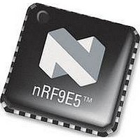
NRF9E5 NORDIC SEMICONDUCTOR, NRF9E5 Datasheet - Page 10

NRF9E5
Manufacturer Part Number
NRF9E5
Description
TRX, 430-928MHZ, MCU/ADC/PWM, SMD
Manufacturer
NORDIC SEMICONDUCTOR
Datasheet
1.NRF9E5.pdf
(108 pages)
Specifications of NRF9E5
Receiving Current
12.5mA
Transmitting Current
30mA
Data Rate
50Kbps
Frequency Range
430MHz To 928MHz
Modulation Type
GFSK
Rf Ic Case Style
QFN
No. Of Pins
32
Supply Voltage Range
1.9V To
Lead Free Status / RoHS Status
Lead free / RoHS Compliant
Available stocks
Company
Part Number
Manufacturer
Quantity
Price
Company:
Part Number:
NRF9E5C
Manufacturer:
NORDIC
Quantity:
5 000
Part Number:
NRF9E5C
Manufacturer:
NORDIC
Quantity:
20 000
PRODUCT SPECIFICATION
nRF9E5 Single Chip Transceiver with Embedded Microcontroller and ADC
1)
2)
3)
4)
5)
6)
7)
8)
9)
10) Conversion rate is dependant on resolution, Please see chapter 10.3 page 32.
Main office: Nordic Semiconductor ASA - Vestre Rosten 81, N-7075 Tiller, Norway -Phone +4772898900 - Fax +4772898989
Revision: 1.3
Symbol Parameter (condition)
RX
RX
C/I
C/I
C/I
C/I
C/I
C/I
C/I
C/I
SFDR
C/I
C/I
C/I
DNL
SNR
SNR
I
INL
V
V
t
V
I
Max value determined by design and characterization testing.
Pin voltages are VSS or VDD.
Higher sink/source current is possible if increased voltage changes on ports are accepted.
Operates in the 433, 868 and 915 MHz ISM band.
The crystal frequency may be chosen from 5 different values (4, 8, 12, 16, and 20MHz) which are specified in
the configuration word. Please see Table 22 on page 38.
Data is Manchester-encoded before GFSK modulation.
Optimum Load Impedance.
Channel width and channel spacing is 200kHz.
Channel Level +3dB over sensitivity, interfering signal a standard carrier wave, Image 2 MHz above wanted.
ADC
NPD
F
RX
+10M
SENS
MAX
-10M
OS
BG
2ND
+1M
+5M
G
FS
-1M
-2M
-5M
1ST
S
CO
IM
Receiver operation
Supply current in receive mode
Sensitivity at 0.1%BER
Maximum received signal
C/I Co-channel
1
2
Blocking at +1MHz
Blocking at -1MHz
Blocking at -2MHz
Blocking at +5MHz
Blocking at -5MHz
Blocking at +10MHz
Blocking at -10MHz
Image rejection
ADC operation
f
Differential Nonlinearity f
Integral Nonlinearity f
Signal to Noise Ratio (without harmonics)
Spurious Free Dynamic Range f
IN
st
nd
Signal to Noise Ratio (DC input)
Midscale offset
Gain Error
Internal reference
Internal reference voltage drift
Reference voltage input (external ref)
Conversion rate
Supply current ADC operation
Start-up time from ADC Power down
adjacent channel selectivity C/I 200kHz
= 10 kHz
adjacent channel selectivity C/I 400kHz
Table 5 nRF9E5 electrical specifications (continued)
IN
= 0.9991 kHz
IN
= 0.9991 kHz
IN
= 10 kHz
Page 10 of 108
Notes
10)
9)
9)
9)
9)
9)
9)
9)
9)
9)
9)
9)
Min.
1.1
0.8
53
0
Typ.
-100
12.5
1.22
100
-16
-40
-50
-63
-70
-65
-69
-67
-36
0.75
13
59
58
65
15
-7
0.5
1
1
1
Max.
125
1.3
1.5
June 2006
ppm/ C
Units
dBFS
dBFS
%FS
%FS
dBm
dBm
LSB
LSB
ksps
mA
mA
dB
dB
dB
dB
dB
dB
dB
dB
dB
dB
dB
dB
V
V
s


