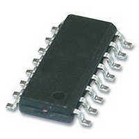
TEA1751LT/N1 NXP Semiconductors, TEA1751LT/N1 Datasheet - Page 25

TEA1751LT/N1
Manufacturer Part Number
TEA1751LT/N1
Description
AC-DC, PFC, FLYBACK, CNTRL, 16SOIC
Manufacturer
NXP Semiconductors
Datasheet
1.TEA1751LTN1518.pdf
(29 pages)
Specifications of TEA1751LT/N1
Input Voltage
276V
Output Current
1.2A
Output Voltage
11V
No. Of Outputs
2
Power Dissipation Pd
600mW
Voltage Regulator Case Style
SOIC
No. Of Pins
16
Operating Temperature Range
-40°C To
Supply Voltage Range
21V To 23V
Rohs Compliant
Yes
Lead Free Status / RoHS Status
Lead free / RoHS Compliant
Available stocks
Company
Part Number
Manufacturer
Quantity
Price
Company:
Part Number:
TEA1751LT/N1
Manufacturer:
SEIKO
Quantity:
55 000
Part Number:
TEA1751LT/N1
Manufacturer:
NXP/恩智浦
Quantity:
20 000
NXP Semiconductors
11. Application information
TEA1751T_LT_2
Product data sheet
A power supply with the TEA1751(L)T consists of a power factor correction circuit
followed by a flyback converter. See
Capacitor C
rectified mains during start-up and via the auxiliary winding of the flyback converter during
operation. Sense resistors R
MOSFETs S1 and S2 into a voltage at pins PFCSENSE and FBSENSE. The values of
R
In the example given, the LATCH pin is connected to a Negative Temperature Coefficient
protection is activated. A capacitor C
120 nF capacitor, typically after 10 ms the time-out protection is activated. R
so that the time-out capacitor does not interfere with the normal regulation loop.
R
normal operation due to negative voltage spikes across the sense resistors.
Resistor R
(NTC) resistor. When the resistance drops below
Fig 17. Typical application diagram TEA1751(L)T
SENSE1
S1
and R
and R
S2
AUX1
VCC
COMPENSATION
are added to prevent the soft start capacitors from being charged during
SENSE2
is added to protect the IC from damage during lightning events.
buffers the IC supply voltage, which is powered via the high voltage
Rev. 02 — 23 December 2009
define the maximum primary peak current in MOSFETs S1 and S2.
R AUX1
R LOOP
C TIMEOUT
8
6
7
3
12
SENSE1
C SS1
11
TEA1751(L)T
R SENSE1
R S1
and R
Figure
TIMEOUT
R SS1
2
TEA1751T; TEA1751LT
SENSE2
S1
D1
16.
9 16 13
is connected to the FBCTRL pin. For a
10
convert the current through the
4
1
5
V
-------------------------------
Θ
I
prot LATCH
O LATCH
R S2
(
(
R SENSE2
GreenChip III SMPS control IC
R SS2
C SS2
C bus
)
)
=
S2
15.6 kΩ
R AUX2
T2
© NXP B.V. 2009. All rights reserved.
C OUT
D2
(typ), the
C VCC
LOOP
014aaa302
is added
25 of 29


