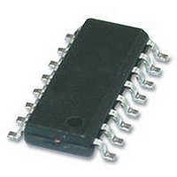
TEA1751LT/N1 NXP Semiconductors, TEA1751LT/N1 Datasheet - Page 11

TEA1751LT/N1
Manufacturer Part Number
TEA1751LT/N1
Description
AC-DC, PFC, FLYBACK, CNTRL, 16SOIC
Manufacturer
NXP Semiconductors
Datasheet
1.TEA1751LTN1518.pdf
(29 pages)
Specifications of TEA1751LT/N1
Input Voltage
276V
Output Current
1.2A
Output Voltage
11V
No. Of Outputs
2
Power Dissipation Pd
600mW
Voltage Regulator Case Style
SOIC
No. Of Pins
16
Operating Temperature Range
-40°C To
Supply Voltage Range
21V To 23V
Rohs Compliant
Yes
Lead Free Status / RoHS Status
Lead free / RoHS Compliant
Available stocks
Company
Part Number
Manufacturer
Quantity
Price
Company:
Part Number:
TEA1751LT/N1
Manufacturer:
SEIKO
Quantity:
55 000
Part Number:
TEA1751LT/N1
Manufacturer:
NXP/恩智浦
Quantity:
20 000
NXP Semiconductors
TEA1751T_LT_2
Product data sheet
7.2.10 Overvoltage protection (VOSENSE pin)
7.2.12 Driver (pin PFCDRIVER)
7.2.11 PFC open loop protection (VOSENSE pin)
7.2.8 Overcurrent protection (PFCSENSE pin)
7.2.9 Mains undervoltage lockout / brownout protection (VINSENSE pin)
The maximum peak current is limited cycle-by-cycle by sensing the voltage across an
external sense resistor, R
measured via the PFCSENSE pin.
To prevent the PFC from operating at very low mains input voltages, the voltage on the
VINSENSE pin is sensed continuously. As soon as the voltage on this pin drops below the
V
The voltage on pin VINSENSE is clamped to a minimum value,
V
restored after a mains dropout.
To prevent output overvoltage during load steps and mains transients, an overvoltage
protection circuit is built in.
As soon as the voltage on the VOSENSE pin exceeds the V
of the power factor correction circuit is inhibited. Switching of the PFC recommences as
soon as the VOSENSE pin voltage drops below the V
When the resistor between pin VOSENSE and ground is open, the overvoltage protection
is also triggered.
The power factor correction circuit does not start switching until the voltage on the
VOSENSE pin is above the V
and VOSENSE short situations.
The driver circuit to the gate of the power MOSFET has a current sourcing capability of
typically −500 mA and a current sink capability of typically 1.2 A. This permits fast turn-on
and turn-off of the power MOSFET for efficient operation.
Fig 6.
stop(VINSENSE)
start(VINSENSE)
Voltage to current transfer function for dual boost PFC
level, switching of the PFC is stopped.
+ ΔV
pu(VINSENSE)
Rev. 02 — 23 December 2009
I
I(VOSENSE)
SENSE1
−15 μA
th(ol)(VOSENSE)
, for a fast restart as soon as the mains input voltage is
, on the source of the external MOSFET. The voltage is
TEA1751T; TEA1751LT
level. This protects the circuit from open loop
2.2 V
ovp(VOSENSE)
V
GreenChip III SMPS control IC
VINSENSE
ovp(VOSENSE)
014aaa097
level again.
© NXP B.V. 2009. All rights reserved.
level, switching
11 of 29


