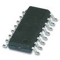
TEA1751LT/N1 NXP Semiconductors, TEA1751LT/N1 Datasheet - Page 24

TEA1751LT/N1
Manufacturer Part Number
TEA1751LT/N1
Description
AC-DC, PFC, FLYBACK, CNTRL, 16SOIC
Manufacturer
NXP Semiconductors
Datasheet
1.TEA1751LTN1518.pdf
(29 pages)
Specifications of TEA1751LT/N1
Input Voltage
276V
Output Current
1.2A
Output Voltage
11V
No. Of Outputs
2
Power Dissipation Pd
600mW
Voltage Regulator Case Style
SOIC
No. Of Pins
16
Operating Temperature Range
-40°C To
Supply Voltage Range
21V To 23V
Rohs Compliant
Yes
Lead Free Status / RoHS Status
Lead free / RoHS Compliant
Available stocks
Company
Part Number
Manufacturer
Quantity
Price
Company:
Part Number:
TEA1751LT/N1
Manufacturer:
SEIKO
Quantity:
55 000
Part Number:
TEA1751LT/N1
Manufacturer:
NXP/恩智浦
Quantity:
20 000
NXP Semiconductors
Table 5.
T
the IC; unless otherwise specified.
[1]
[2]
[3]
[4]
[5]
TEA1751T_LT_2
Product data sheet
Symbol
t
Soft start flyback (pin FBSENSE)
I
V
R
Overcurrent protection flyback (pin FBSENSE)
V
t
I
I
Driver (pin FBDRIVER)
I
I
V
LATCH input (pin LATCH)
V
I
V
V
V
Temperature protection
T
T
d(vrec-swon)
start(soft)fb
leb(fb)
start(OPP)FBAUX
opp(red)(FBAUX)
src(FBDRIVER)
sink(FBDRIVER)
O(LATCH)
amb
pl(IC)
pl(IC)hys
start(soft)fb
sense(fb)max
O(FBDRIVER)(max)
prot(LATCH)
en(LATCH)
hys(LATCH)
oc(LATCH)
start(soft)fb
For a typical application with a compensation network on pin PFCCOMP, like the example in
Minimum required voltage change time for valley recognition on pin PFCAUX.
Minimum time required between demagnetization detection and ΔV/Δt = 0 on pin PFCAUX.
Hysteresis for PFC on/off control.
Guaranteed by design.
= 25
°
C; V
Characteristics
CC
= 20 V; all voltages are measured with respect to ground (pin 2); currents are positive when flowing into
Parameter
valley recognition to switch-on
delay time
flyback soft start current
flyback soft start voltage
flyback soft start resistance
maximum flyback sense
voltage
flyback leading edge blanking
time
OPP start current on pin
FBAUX
reduced overpower protection
current on pin FBAUX
source current on pin
FBDRIVER
sink current on pin FBDRIVER V
maximum output voltage on pin
FBDRIVER
protection voltage on pin
LATCH
output current on pin LATCH
enable voltage on pin LATCH
hysteresis voltage on pin
LATCH
open-circuit voltage on pin
LATCH
IC protection level temperature
hysteresis of IC protection level
temperature
…continued
Rev. 02 — 23 December 2009
Conditions
enable voltage
ΔV/Δt = 50 mV/μs
ΔV/Δt = 200 mV/μs
V
0.37 V
V
V
V
at start-up
V
sense(fb)max
FBDRIVER
FBDRIVER
FBDRIVER
prot(LATCH)
en(LATCH)
− V
= 2 V
= 2 V
= 10 V
< V
has reduced to
prot(LATCH)
LATCH
TEA1751T; TEA1751LT
< V
oc(LATCH)
Figure
GreenChip III SMPS control IC
[5]
3.
Min
-
−75
0.43
12
0.49
0.52
255
-
-
-
-
-
-
1.23
−85
1.30
80
2.65
130
-
Typ
150
−60
0.52
0.55
305
−100
−360
−0.5
0.7
11
1.25
−80
1.35
100
2.9
140
10
0.49
-
1.2
© NXP B.V. 2009. All rights reserved.
Max
-
−45
0.54
-
0.55
0.58
355
-
-
-
-
-
12
1.27
−75
1.40
140
3.15
150
-
Unit
ns
μA
V
kΩ
V
V
ns
μA
μA
A
A
A
V
V
μA
V
mV
V
°C
°C
24 of 29


