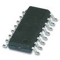
TEA1751LT/N1 NXP Semiconductors, TEA1751LT/N1 Datasheet - Page 21

TEA1751LT/N1
Manufacturer Part Number
TEA1751LT/N1
Description
AC-DC, PFC, FLYBACK, CNTRL, 16SOIC
Manufacturer
NXP Semiconductors
Datasheet
1.TEA1751LTN1518.pdf
(29 pages)
Specifications of TEA1751LT/N1
Input Voltage
276V
Output Current
1.2A
Output Voltage
11V
No. Of Outputs
2
Power Dissipation Pd
600mW
Voltage Regulator Case Style
SOIC
No. Of Pins
16
Operating Temperature Range
-40°C To
Supply Voltage Range
21V To 23V
Rohs Compliant
Yes
Lead Free Status / RoHS Status
Lead free / RoHS Compliant
Available stocks
Company
Part Number
Manufacturer
Quantity
Price
Company:
Part Number:
TEA1751LT/N1
Manufacturer:
SEIKO
Quantity:
55 000
Part Number:
TEA1751LT/N1
Manufacturer:
NXP/恩智浦
Quantity:
20 000
NXP Semiconductors
Table 5.
T
the IC; unless otherwise specified.
TEA1751T_LT_2
Product data sheet
Symbol
V
V
V
I
I
I
Input voltage sensing PFC (pin VINSENSE)
V
V
ΔV
I
V
V
V
I
V
Loop compensation PFC (pin PFCCOMP)
g
I
V
V
V
Pulse width modulator PFC
t
ch(low)
ch(high)
CC(oper)
pu(VINSENSE)
I(VINSENSE)
O(PFCCOMP)
on(PFC)
amb
m
th(UVLO)
start(hys)
hys
stop(VINSENSE)
start(VINSENSE)
mvc(VINSENSE)max
flr
flr(hys)
bst(dual)
clamp(PFCCOMP)
ton(PFCCOMP)zero
ton(PFCCOMP)max
pu(VINSENSE)
= 25
°
C; V
Characteristics
CC
= 20 V; all voltages are measured with respect to ground (pin 2); currents are positive when flowing into
Parameter
undervoltage lockout threshold
voltage
hysteresis of start voltage
hysteresis voltage
low charging current
high charging current
operating supply current
stop voltage on pin VINSENSE
start voltage on pin VINSENSE
pull-up voltage difference on
pin VINSENSE
pull-up current on pin
VINSENSE
maximum mains voltage
compensation voltage on pin
VINSENSE
fast latch reset voltage
hysteresis of fast latch reset
voltage
input current on pin VINSENSE V
dual boost voltage
transconductance
output current on pin
PFCCOMP
clamp voltage on pin
PFCCOMP
zero on-time voltage on pin
PFCCOMP
maximum on-time voltage on
pin PFCCOMP
PFC on-time
…continued
Rev. 02 — 23 December 2009
Conditions
during start-up phase
V
V
V
V
no load on pin FBDRIVER and
PFCDRIVER
active after V
detected
active after V
detected
active after V
V
current switch-over point
switch-over region
V
V
V
Low power mode; PFC off; lower
clamp voltage
Upper clamp voltage
V
V
V
V
startup
HV
th(UVLO)
HV
VINSENSE
start(VINSENSE)
VOSENSE
VOSENSE
VOSENSE
VINSENSE
PFCCOMP
VINSENSE
PFCCOMP
> 80 V; V
> 80 V; V
− V
< V
= 3.3 V
= 2.0 V
to I
= V
= V
th(UVLO)
> V
= 3.3 V;
= 0.9 V;
CC
stop(VINSENSE)
stop(VINSENSE)
th(UVLO)
O(PFCCOMP)
CC
trip
stop(VINSENSE)
ton(PFCCOMP)max
ton(PFCCOMP)max
is detected
< V
< V
< V
TEA1751T; TEA1751LT
startup
CC
trip
is detected
< V
or
th(UVLO)
is
is
after
[1]
[1]
GreenChip III SMPS control IC
Min
14
-
6.3
−1.2
−4.6
2.25
0.86
1.11
-
−55
4.0
-
-
5
-
-
60
33
−45
2.5
-
3.4
1.20
3.6
30
Typ
15
300
7
−1.0
−5.4
3
0.89
1.15
−100
−47
-
0.75
0.12
33
80
39
−39
2.7
3.9
3.5
1.25
4.5
40
2.2
200
© NXP B.V. 2009. All rights reserved.
Max
16
-
7.7
−0.8
−6.3
3.75
0.92
1.19
-
−40
-
-
-
100
-
-
100
45
−33
2.9
-
3.6
1.30
5.0
53
Unit
V
mV
V
mA
mA
mA
V
V
mV
μA
V
V
V
nA
V
mV
μA/V
μA
μA
V
V
V
V
μs
μs
21 of 29


