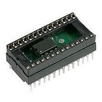
NTE21128 NTE ELECTRONICS, NTE21128 Datasheet - Page 4

NTE21128
Manufacturer Part Number
NTE21128
Description
IC, EPROM, 128KBIT, 250NS, DIP-28
Manufacturer
NTE ELECTRONICS
Datasheet
1.NTE21128.pdf
(6 pages)
Specifications of NTE21128
Memory Type
EPROM - OTP
Memory Size
128Kbit
Memory Configuration
16K X 8
Access Time
250ns
Supply Voltage Range
4.75V To 5.25V
Memory Case Style
DIP
No. Of Pins
28
Two Line Output Control
The NTE21128 features a 2 line control function which accommodates the use of multiple memory
connection. The two line control function allows:
For the most efficient use of these two control lines, E should be decoded and used as the primary
device selecting function, while G should be made a common connection to all devices in the array
and connected to the READ line from the system control bus.
This ensures that all deselected memory devices are in their low power standby mode and that the
output pins are only active when data is required from a particular memory device.
System Considerations
The power switching characteristics of EPROMs require careful decoupling of the devices. The sup-
ply current (I
level, the active current level, and transient current peaks that are produced by the falling and rising
edges of E. The magnitude of these transient current peaks is dependent on the capacitive and induc-
tive loading of the device at the output. The associated transient voltage peaks can be suppressed
by complying with the two line output control and by properly selecting decoupling capacitors. It is
recommended that a 1 f ceramic capacitor be used on every device between V
should be a high frequency capacitor of low inherent inductance and should be placed as close to the
device as possible. In addition, a 4.7 f bulk electrolytic capacitor should be used between V
GND for every eight devices. The bulk capacitor should be located near the power supply connection
point. The purpose of the bulk capacitor is to overcome the voltage drop caused by the inductive ef-
fects of PCB traces.
Programming
When delivered, all bits of the NTE21128 are in the “1” state. Data is introduced by selectively pro-
gramming “0s” into the desired bit locations. Although only “0s” will be programmed, both “1s” and
“0s” can be present in the data word. The only way to change a “0” to a “1” is by ultraviolet light erasure.
The NTE21128 is in the programming mode when the V
low. The data to be programmed is applied 8 bits in parallel to the data output pins. The levels required
for the address and data inputs are TTL.
Fast Programming Algorithm
Fast Programming Algorithm rapidly programs the NTE21128 EPROM using an efficient and reliable
method suited to the production programming environment. Programming reliability is also ensured
as the incremental program margin of each byte is continually monitored to determine when it has
been successfully programmed. The Fast Programming Algorithm utilizes two different pulse types:
initial and overprogram.
The duration of the initial P pulse(s) is 1ms, which will then be followed by a longer overprogram pulse
of length 3ms by n (n is equal to the number of the initial one–millisecond pulses applied to a particular
NTE21128 location), before a correct verify occurs. Up to 25 one–millisecond pulses per byte are
provided for before the over program pulse is applied.
The entire sequence of program pulses and byte verifications is performed at V
12.5V. When the Fast Programming cycle has been completed, all bytes should be compared to the
original data with V
CC
a.
b.
) has three segments that are of interest to the system designer: the standby current
CC
= 5V and V
the lowest possible memory power dissipation,
complete assurance that output bus contention will not occur.
PP
= 5V.
PP
input is at 12.5V and E and P are at TTL
CC
CC
= 6V and V
and V
SS
CC
. This
PP
and
=


