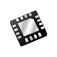
MMA5206WR2 Freescale Semiconductor, MMA5206WR2 Datasheet - Page 58

MMA5206WR2
Manufacturer Part Number
MMA5206WR2
Description
IC ACCELER 60G X-AXIS 16QFN
Manufacturer
Freescale Semiconductor
Datasheet
1.MMA5206WR2.pdf
(63 pages)
Specifications of MMA5206WR2
Sensing Axis
X
Acceleration
60 g
Sensitivity
0.125 g/LSB
Package / Case
QFN-16
Supply Voltage (max)
25 V
Supply Current
4 mA to 8 mA
Maximum Operating Temperature
+ 125 C
Minimum Operating Temperature
- 40 C
Mounting Style
SMD/SMT
Lead Free Status / RoHS Status
Lead free / RoHS Compliant
58
6.3
register data write and read operations. Two register pointer operations are provided: Register Pointer Write, and Register Pointer
Read. Command and response information is shown in
6.4
contained in the register pointer.
6.4.1
contain the data to be written to the register pointed to by the register pointer. The least significant 8 bits of the Register Write
response message contain the address of the register that was modified.
6.4.2
are ignored. The least significant 8 bits of the Register Read response message contain the contents of the register pointed to
by the register pointer.
ically be frozen on a read of the low byte of the register.
6.4.3
10-bit acceleration data depending on the state of the DATASIZE bit in the DEVCFG2 register.
6.4.4
6.4.4.1
6.4.4.2
to the subsequent message with the Parity Fault response, as shown in
6.4.5
MMA52xxWR
Access to internal registers is accomplished via a pointer register. The pointer contains the address of the register affected by
Two register operations are provided: Register Write, and Register Read. In each case, the address of the affected register is
The Register Write command format is shown in
The write to the register is executed during the clock cycle immediately after CS is de-asserted.
The Register Read command format is shown in
16-bit register reads are possible using consecutive Register Read commands. The high byte of a 16-bit register will automat-
The Acceleration Data Read command format is shown in
Reference
If the device detects a Command Parity fault, the current, and subsequent SPI commands are ignored and the device responds
DATASIZE = 1 (10-Bit Data)
DATASIZE = 0 (8-Bit Data)
Register Pointer Operations
Register Data Operations
Register Write Command
Register Read Command
Acceleration Data Read Operations
Error Responses
SPI OTP Programming Procedure
1. Set V
2. Enter SPI DPM.
3. Load desired data into the OTP shadow registers using SPI Write commands.
4. Write 0x05 to register $44 to initiate the NVM programming.
5. Read the SC register and verify IDEF_B flag is set (indicating the write is complete and successful).
6. Reset the device.
7. Re-entering SPI DPM.
8. Read the OTP register values and compare to the desired values.
DATASIZE
Table 20
Response to Invalid Commands
Parity Fault Response
a.
CC
= V
for responses to Invalid Commands.
OTP write time depends on the number of bits being written to ‘1’. Each bit that is programmed
requires t
PP
.
PROG_BIT
D15 D14 D13 D12 D11 D10
1
1
.
0
0
0
0
Table
Table
Table
1
1
20. The least significant 8 bits of the Register Write command message
20. The least significant 8 bits of the Register Read command message
Table
1
1
20.
P
P
20. The response to this command provides either 8-bit, or
D9
D9
Table
0
D8
D8
0
20.
Bit
D7
D7
D7
D6
D6
D6
D5
D5
D5
D4
D4
D4
Freescale Semiconductor
D3
D3
D3
D2
D2
D2
D1
D1
D1
Sensors
D0
D0
D0


