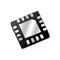
MMA5206WR2 Freescale Semiconductor, MMA5206WR2 Datasheet - Page 56

MMA5206WR2
Manufacturer Part Number
MMA5206WR2
Description
IC ACCELER 60G X-AXIS 16QFN
Manufacturer
Freescale Semiconductor
Datasheet
1.MMA5206WR2.pdf
(63 pages)
Specifications of MMA5206WR2
Sensing Axis
X
Acceleration
60 g
Sensitivity
0.125 g/LSB
Package / Case
QFN-16
Supply Voltage (max)
25 V
Supply Current
4 mA to 8 mA
Maximum Operating Temperature
+ 125 C
Minimum Operating Temperature
- 40 C
Mounting Style
SMD/SMT
Lead Free Status / RoHS Status
Lead free / RoHS Compliant
56
6
the SPI transfer protocol.
6.0.1
6.0.2
bit is located in bit D10, and the parity is calculated using bits D15 through D11. For Write commands, the parity bit is located in
bit D9, and the parity is calculated using bits D15 through D0. If a parity error is detected, both the current and subsequent com-
mands are ignored, and the parity fault response is transmitted during the subsequent SPI transfer.
6.0.3
16-bit message.
MMA52xxWR
SPI Diagnostic and Programming Mode allows for the following functions:
SPI transfers follow CPOL = 0, CPHA = 0, MSB first convention.
The following operations are supported in DPM:
All commands except for the DPM Entry command employ odd parity to ensure data integrity. For Read commands, the parity
All responses except for the DPM entry response employ odd parity to ensure data integrity. Parity is calculated using the entire
SCLK
D
OUT
BIT
D
CS
IN
SPI DIAGNOSTIC AND PROGRAMMING MODE
Communication Error Detection
Data Input Parity Detection
Data Output Parity
•
•
• Register pointer write
• Register pointer read
• Register data write
• Register data read
• Acceleration data read
D15
15
D15
Programming of the OTP array
Reading of memory registers
D14
14
D14
D13
13
D13
D12
D12
12
D11
D11
11
Figure 45. SPI Transfer Protocol
D10
D10
10
D9
D9
9
D8
D8
8
Figure 7
D7
D7
7
shows the SPI transfer timing, and
D6
D6
6
D5
D5
5
D4
D4
4
D3
D3
3
Freescale Semiconductor
D2
D2
2
Figure 45
D1
D1
1
0
D0
D0
Sensors
shows


