MMA5206WR2 Freescale Semiconductor, MMA5206WR2 Datasheet
MMA5206WR2
Specifications of MMA5206WR2


Related parts for MMA5206WR2

MMA5206WR2 Summary of contents
Page 1
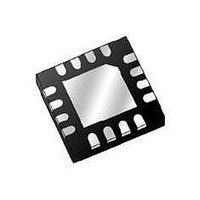
... Airbag Front and Side Crash Detection ORDERING INFORMATION Temperature Device Axis Range MMA5206W X 60g MMA5212W X 120g MMA5224W X 240g MMA5248W X 480g MMA5206WR2 X 60g MMA5212WR2 X 120g MMA5224WR2 X 240g MMA5248WR2 X 480g © Freescale Semiconductor, Inc., 2010. All rights reserved. Package Shipping I DATA 2086-01 ...
Page 2
... CC 27 Ω, 5%, 200 PPM I Filtering and Signal Damping DATA 20 kΩ, 5%, 200 PPM Gate Resistor for External Low Side Daisy Chain FET — Low Side Daisy Chain Transistor xxxxxxx xxxxxxx -1g EARTH GROUND Figure 2. Device Orientation Diagram SS_OUT Purpose Sensors Freescale Semiconductor ...
Page 3
... V Buffer CC Voltage Regulator Reference Voltage CS SCLK SPI OUT V Self-Test Interface V V REGA REG g-cell ΣΔ Converter Sensors Freescale Semiconductor V BUF Digital V Voltage Regulator V REF Analog V Voltage Regulator Control Logic OTP Array REG Status Control Out In DSP IIR LPF SINC Filter Compensation Figure 3 ...
Page 4
... Figure 1. SSA ) supplies to provide immunity from EMC and supply dropouts Reference Figure Reference SS SS_OUT. SSA REGA REG external capacitor must be connected CC Figure 1. If unused, this pin must be left unconnected. Section 7 for die attach pad connection details. Freescale Semiconductor ) and REGA Sensors ...
Page 5
... K/min, unless otherwise specified Characteristic Supply Voltage 16 17 ≤ 85 mA) Programming Voltage (I DATA 18 Applied DATA, CC Operating Temperature Range 19 Sensors Freescale Semiconductor Symbol V CC_REV V CC_MAX V CC_TRANS -0.3 to +4.2 -0.3 to +3.0 g pms g shock h DROP V ESD V ESD V ESD V ESD T -40 to +125 stg ...
Page 6
... V REG -100 — -10 10 — 100 20 æ 100 — — -55 155 — — 3.15 — V BUF 0.0 — 0.45 — t — S-S_PM_L — — 300 200000 / f OSC Freescale Semiconductor mA (1) mA (1) mA (3) V (1) V (1) V ( (3) V (3) V (3) V (3) nF (9) (9) V (3, 11) ...
Page 7
... Range Positive/Negative ΣΔ and Sinc Filter Clipping Limit 84 ±120g Range Positive/Negative ΣΔ and Sinc Filter Clipping Limit 85 ±240g Range Positive/Negative ΣΔ and Sinc Filter Clipping Limit 86 ±480g Range Positive/Negative Sensors Freescale Semiconductor Symbol * SENS * SENS * SENS * SENS ΔSENS_240 * Δ ...
Page 8
... OSC OSC — OSC OSC μs 495 500 505 μs — — S-S_PM μs — — 20 — — μs 512 — — Freescale Semiconductor (7) (7) (7) (7) (7) (7, 12) (7, 12) (7, 12) (7, 12) (7) (7) (7) (7) (7) (7, 12) (7) (7) (7) (7) (7) (9) (7) (7) (7) (9) (7) (7) (7) (7) ...
Page 9
... Sensing Element Damping Ratio 166 ±60g 167 ±120g 168 ±240g 169 ±480g Sensing Element Delay (@100Hz) 170 ±60g 171 ±120g 172 ±240g 173 ±480g Package Resonance Frequency 174 Sensors Freescale Semiconductor Symbol Min Typ * f 3.80 4 OSC ⎯ 400 C_LPF0 ⎯ LPF0 ⎯ * ...
Page 10
... LEAD ⎯ ⎯ 60 ⎯ ⎯ 20 ⎯ ⎯ 10 ⎯ ⎯ 0 ⎯ ⎯ 50 ⎯ ⎯ LAG ⎯ ⎯ 60 ⎯ ⎯ 1000 CSN Freescale Semiconductor Units ms (3) s (7) μs (3) μs (3) μs (3) s (7) s (7) s (7) s (7) s (7) s (7) s (7) ns (9) ns (9) ns (9) ns ...
Page 11
... POR CS t SCLKR t LEAD t SCLK SCLK t SCLKL t ACCESS t VALID D OUT t HOLD_IN t SETUP D IN Sensors Freescale Semiconductor t S-S t SYNC Figure 5. Sync Pulse Characteristics Response Terminated if in process Time Figure 6. Power-Up Timing t SCLKF t SCLKH t HOLD_OUT Figure 7. Serial Interface Timing V IDLE t CSN t LAG t DISABLE ...
Page 12
... SN[9] SN[8] SN[19] SN[18] SN[17] SN[16] SN[27] SN[26] SN[25] SN[24] 0 RNG[2] RNG[1] RNG[0] DATASIZE BLANKTIME P_CRC BAUD U_REV[3] U_REV[2] U_REV[1] U_REV[0] YEAR[3] YEAR[2] YEAR[1] YEAR[0] DAY[3] DAY[2] DAY[1] DAY[0] OC_INIT_B IDEF_B OFF_B TEMPF_B Section 3.2.1 Freescale Semiconductor Type for details Sensors ...
Page 13
... The PCM bit enables the PCM output pin. When the PCM bit is set, the PCM output pin is active and outputs a Pulse Code Modulated signal proportional to the acceleration response. Reference output. When the PCM bit is cleared, the PCM output pin is actively pulled low. Sensors Freescale Semiconductor Bit 6 5 ...
Page 14
... Synchronous Sampling Mode (Latency relative to Time Slot) DATASIZE Data Length 0 10 Bits 1 8 Bits Blanking Time Method Maximum Response Transmission Complete SYNC_OFF_500 for details regarding response message error detection. P_CRC Parity or CRC 0 Parity 1 CRC Sync Pulse Pull-Down x Disabled x Enabled x Disabled No Disabled Yes Enabled Sensors Freescale Semiconductor ...
Page 15
... PSI5 Version 1.3 specification, or time slots which will cause data contention. TIMESLOTx[9:0] ASYNC Bit 0 00 0000 0000 1 Non-Zero N/A Note: TIMESLOTB is only used for Synchronous Double Sample Rate Mode and 16-Bit Resolution Mode. Sensors Freescale Semiconductor BAUD Baud Rate 0 Low Baud Rate (125 kBaud) 1 High Baud Rate (190.5 kBaud) Bit ...
Page 16
... Bushing Direction (α) Perpendicular to α and β (γ) Not used U_REV[3] U_REV[2] U_REV[1] YEAR[3] YEAR[2] YEAR[1] DAY[3] DAY[2] DAY[ Section 4.4.2.1 Section 3.1.4.3. Section 4.4.2.1. PSI5 Init Data Transmission (D8) Reference Table 12 0000 0100 1000 1100 Freescale Semiconductor 0 U_REV[0] YEAR[0] DAY[0] 0 Sensors ...
Page 17
... User Configuration CRC (CRC_U[2:0]) The user configuration CRC bits contain the 3-bit CRC used for verification of the user programmable OTP array. Reference Section 3.2.2 for information regarding the CRC for the user programmable OTP array. Sensors Freescale Semiconductor Decoded Value Year 2009 • ...
Page 18
... Offset Cancellation in initialization Offset Cancellation initialization complete (t Error Condition CRC error in factory programmable OTP array No error detected Error Condition Offset error detected No error detected Error Condition Over- or Under-Temperature error condition detected No error detected IDEF_B OFF_B TEMPF_B and t expired) OC1 OC2 Freescale Semiconductor 0 Sensors ...
Page 19
... The calculated CRC is then compared against the CRC_U[2:0] bits CRC mismatch is detected, the IDEN_B bit is cleared in the SC register. The CRC verification is completed on the memory registers which hold a copy of the fuse array values, not the fuse array val- ues. Sensors Freescale Semiconductor with a seed with a seed value = ‘111’. The calcu- ...
Page 20
... COMPARATOR V BUF COMPARATOR V REG COMPARATOR V REGA COMPARATOR V REF Figure 8. Voltage Regulation and Monitoring ) to provide BUF Figure 2.50 V REGA V BIAS OSCILLATOR GENERATOR TRIM TRIM ΣΔ CONVERTER V = 1.250 V REF_MOD OTP ARRAY = 2. DIGITAL LOGIC DSP Micro-cut POR Freescale Semiconductor BUF REGA REG Sensors ...
Page 21
... BUF V REG V REGA Response Terminated I DATA POR Sensors Freescale Semiconductor Regulator Capacitor Figure 1 shows the recommended types and values for each of these capacitors. Undervoltage Monitor REGA ) and all internally regulated voltages (V CC undervoltage detected Time Figure 9. V Micro-Cut Response and the as- ...
Page 22
... CAPTEST_ADLY seconds after each sync pulse for a duration of CAPTEST_SDLY CAPTEST_RATE t CAPTEST_ADLY Capacitor Open Time Capacitor Monitor - Asynchronous Mode BUF t CAPTEST_TIME t TRIG Time Capacitor Monitor - Synchronous Mode BUF , ca- BUF REG REGA ), for a duration of t seconds. CAPTEST_TIME t CAPTEST_SDLY Capacitor Open Sensors Freescale Semiconductor ...
Page 23
... CAP_Test V REG V PORVREG_f POR CAP_Test V REGA V PORREGA_f POR 3.4 Internal Oscillator A factory trimmed oscillator is included as specified in Sensors Freescale Semiconductor t CAPTEST_RATE t CAPTEST_TIME Capacitor Present Time Figure 12. V Capacitor Monitor REG t CAPTEST_RATE t CAPTEST_TIME Capacitor Present Time Figure 13. V Capacitor Monitor REGA Section 2. Capacitor Open ...
Page 24
... FIRST SECOND INTEGRATOR INTEGRATOR α β β ±2 × V Figure 14. ΣΔ Converter Block Diagram Figure 15 COMPENSATION OFFSET CANCELLATION F OUTPUT RATE LIMITING Figure 15. Signal Chain Diagram 1-BIT QUANTIZER -1 ΣΔ_OUT -1 ADC DAC REF OUTPUT H G OUTPUT SCALING INTERPOLATION Sensors Freescale Semiconductor ...
Page 25
... Output Scaling H Interpolation 1 3.5.3.1 Decimation Sinc Filter The serial data stream produced by the ΣΔ converter is decimated and converted to parallel values by a 3rd order 16:1 sinc filter with a decimation factor of 16. Sensors Freescale Semiconductor Data Over Signal Signal Signal Width Range Width ...
Page 26
... Response parameters for the low-pass filter are specified in Figure 17 and Figure 18. Filter Coefficients -9.481076477495780e- -1.915847097557409e+ 9.191065266874253e- -1.892328151433503e+ 8.954713774195870e- -1.918978239761011e+ 9.229853042218408e- – – ⋅ ⋅ ⋅ ⋅ ⋅ – ⋅ – ) Group Delay 1.0 0 2816/f 1.0 1.0 3392/f 1.0 Freescale Semiconductor Sec- osc osc Sensors ...
Page 27
... Figure 17. Low-Pass Filter Characteristics: f Sensors Freescale Semiconductor = 16 μs = 400 Hz, 4-Pole MMA52xxWR 27 ...
Page 28
... Figure 18. Low-Pass Filter Characteristics: f MMA52xxWR μs = 400 Hz, 3-Pole Freescale Semiconductor Sensors ...
Page 29
... OFF LSB every t Step_xx Table 5. Offset Cancellation Start-up Characteristics and Timing Offset Cancellation Offset LPF Start-Up Phase 0.3 Hz Self-Test 0.3 Hz Complete 0.1 Hz Sensors Freescale Semiconductor INC/DEC ) COUNTER ) 0.5 Hz (Derived from f ) OSC CLK OFFMON NEG INC/DEC OFFMON POS CLK 2 kHz (Derived from f ...
Page 30
... Figure 21. 0.1 Hz Offset Cancellation Low Pass Filter Characteristics MMA52xxWR 30 Coefficients 0.015956938266754 0.499998132328277 do 1 0.499998132328277 do -0.984043061733246 2 0.000482380390167 0.499938218213271 do 1 0.499938218213271 do -0.999517619609833 2 0.0001608133316040 0.4999999403953552 do 1 0.4999999403953552 do -0.9998391270637512 2 0.0000643134117126 0.4999999403953552 do 1 0.4999999403953552 do -0.9999356269836426 2 Group Delay 1.0 16.384 ms 1.0 537.6 ms 1.0 1591ms 1.0 3976ms Sensors Freescale Semiconductor ...
Page 31
... PCM pin. The PCM output is intended for test use only. D[21:13] 9 Output Scaling Section 3.5.3.6 Sample updated every 16μS Figure 23. PCM Output Function Block Diagram Sensors Freescale Semiconductor Section 2.4. An up/down counter is employed to count up If the output ). The offset monitor is disabled during Initialization Phase1, Phase 2, and CNTSIZE Signal D18 D17 ...
Page 32
... MMA52xxWR 32 g-cell Rolloff LPF Rolloff Region of No Signal Distortion Beyond Specification f g-Cell Figure 24. Output Clipping Vs. Frequency Determined by g-cell roll-off and ADC clipping Determined by g-cell roll-off and full scale range 5kHz 10kHz Frequency (kHz) Section The DSP operates ADC_CLIP Sensors Freescale Semiconductor ...
Page 33
... Upon reception of a synchronization pulse, the device delays a specified period of time, called a time slot, before transmitting acceleration data. For more details regarding time slots, refer to + ΔV V IDLE SYNC V IDLE GND IDLE MOD I IDLE Figure 26. Synchronous Communication Overview Sensors Freescale Semiconductor Figure 25 SATELLITE MODULE # CC_OUT V SS_OUT SATELLITE MODULE # ...
Page 34
... Once the comparator output goes high, all of the internal OSC ), and initiates the timers associated with TRIG SYNC_OFF R CONTROL SYNC_DET LOGIC SYNC_LPF_RESET exceeds V ). The comparator output SYNC_REF ). If the counter is above the limit, a valid SYNC ). user TRIG SYNC_OFF Section 2.6 for timing + (2+DATASIZE+(P_CRC?3:1)) SYNC_LPF_RESET). sample. SYNC_DET Freescale Semiconductor Sensors ...
Page 35
... If consecutive “1” or “0” data are transmitted, There will also be a transition at the start of a bit time. I CURRENT MOD IDLE CURRENT CONSECUTIVE ‘0’ DATA BITS CONSECUTIVE ‘1’ DATA BITS Sensors Freescale Semiconductor t PD_DLY t PD_ON t SYNC_LPF_RST t SYNC_OFF_xxx t TIMESLOTx ...
Page 36
... MMA52xxWR ‘1’ ‘1’ ‘0’ ‘0’ ‘1’ ‘1’ (2+DATASIZE+(P_CRC?3:1)) TRAN = BIT t FRAME Data Transmitted Figure 30 PAR SB1 ‘1’ ‘1’ ‘0’ ‘1’ calculation.Table 7 shows some example CRC CRC Freescale Semiconductor Sensors ...
Page 37
... Sensors Freescale Semiconductor 10-Bit Data Value Hex +511 $1FF • • • • Reserved • • +502 $1F6 +501 $1F5 +500 $1F4 Sensor Defect Error Message ...
Page 38
... Device Initialization • Program Mode Entry Verification • Offset Cancellation Initialization (2 Stages) • Self-Test Figure 32 shows the timing for internal and external initialization. MMA52xxWR 38 ... INIT 1 INIT 3 INIT 2 Figure 31. PSI5 Sensor 10-Bit Initialization Normal Mode Sync Pulses NORMAL MODE Freescale Semiconductor Sensors ...
Page 39
... OC1 INT_INIT Programming Mode Entry 1) Min. 31 sync pulses Sync 2) PME command Pulses Otherwise Ignored Sync Pulses Ignored t t PME RS_PM Sensors Freescale Semiconductor PSI5 Initialization Phase 2 t PSI5_INIT2 Self-Test Self-Test Raw Offset Deflection Normal Data Stage 2 Calculation Verification OC2 ST1 ...
Page 40
... ID1L D1L D1L ... D1L Repeat k times × × ( TRANS NIBBLE k DataFields = ) Table 12, and in the order shown in ... D32 D2 ... ID32 D32 ID32 D32 ... ... Repeat k times ... D9 ID9L ID9L ... D9L D9L ... ... Repeat k times ) × – Freescale Semiconductor ) PSI5_INIT2 ID32 D32 k k ID9L D9L k k Sensors ...
Page 41
... Offset and average self-test data will only be transmitted with sync pulse periods that guarantee the self-test phase1 & phase 2 will be complete prior to required transmission. If sync pulse periods faster than this are used, ‘0’s will be transmitted instead of offset and/or average self-test data. Sensors Freescale Semiconductor Table 9 and Table 10 ...
Page 42
... Number of Data Blocks = 9 Number of Data Blocks = 9 Number of Data Blocks = 9 Satellite Manufacturer = Freescale Satellite Manufacturer = Freescale Satellite Manufacturer = Freescale Satellite Manufacturer = Freescale Sensor Type = Acceleration (high g) Sensor Type = Acceleration (high g) Sensor Type = Acceleration (high g) Sensor Type = Acceleration (high g) Axis Range Freescale Semiconductor Value ...
Page 43
... Initialization Phase 3 times for different operating modes and self-test repeats. Times are calcu- lated using the following equation ⎛ INTINIT OC1 ROUNDUP -------------------------------------------------------------------------------------------------------------------------------------------------------------------------------------------------------------------------------------------- - = ⎝ PSI5INIT3 Sensors Freescale Semiconductor (Self-Test Disabled). ST1 + 2ms ST2 ST2 ST3 Table 8. The number of messages transmitted in initialization phase ( ) × ...
Page 44
... Nominal Phase 3 Defect Messages Time (ms) 0.46 86.18 182.17 278.16 374.15 470.14 4.79 100.78 196.76 292.75 388.74 484.73 2 1.00 74.00 170.00 266.00 362.00 458.00 1.00 90.00 186.00 282.00 378.00 474.00 Sensors Freescale Semiconductor ...
Page 45
... Mode”, and by programming the LATENCY bit to “Simultaneous Sampling Mode”. In Simultaneous Sampling Mode, the most recent interpolated acceleration data sample is latched at t Pulse) and transmitted starting at the time programmed in TIMESLOTA[9:0], relative to t Sensors Freescale Semiconductor ) and will not respond to normal sync pulses. However, ASYNC Figure 35. Simultaneous Sampling Mode ...
Page 46
... In Synchronous Sampling Mode, the most recent interpolated acceleration data sample is latched at the time programmed in TIMESLOTA[9:0], relative to t (rising edge of Sync Pulse). The data is transmitted starting at the time programmed in TIMES- TRIG LOTA[9:0], relative TRIG Figure 36. Synchronous Sampling Mode with Minimum Latency MMA52xxWR 46 ≤ LAT_INTERP DATASETUP_synch t TIMESLOTA Freescale Semiconductor Sensors ...
Page 47
... Figure 37. Synchronous Double Sample Rate Mode Note: In the event that the programmed values in TIMESLOTA [9:0] transmitted in TIMESLOTB Sensors Freescale Semiconductor (rising edge of Sync Pulse). This data is transmitted starting at the time pro- TRIG . In addition, the most recent interpolated acceleration data sample is latched at TRIG ...
Page 48
... Figure 38. 16-Bit Output Scaling Diagram (rising edge of Sync Pulse). In Synchronous Sampling Mode, the most recent inter- TRIG . TRIG ≤t LAT_INTERP [9:0] and TIMESLOTB . Figure 38 shows the method Margin ... Using Rounding (rising edge of Sync TRIG + t DATASETUP_16 [9:0] result in a conflict, no data will be Freescale Semiconductor D1 D0 Sensors ...
Page 49
... Global Address for Broadcast Message to all Sensors Sensors Freescale Semiconductor . Table 15. Table 16. Table 14 and Table 15. Reference Section 3.1.4.3 Default time slot specified in Section 3.1.3.5 Section 3.1.3.7 Section 3.1.3.8 Low Baud Rate: 125 kBaud Command F0 A0 Set Sensor Address (Daisy Chain) 0 Broadcast Message - “Run Mode” ...
Page 50
... Temporary (Normal transmissions continue once offset returns within limits) Error Type Temporary: Normal transmissions continue once voltage returns above failure limit) Temporary: Normal transmissions continue once temperature returns within the specified limits) Error Type Latched until reset Latched until reset Freescale Semiconductor Sensors ...
Page 51
... The device responds only to valid PSI5 Short and Long Commands addressed to Sensor Address ‘001’, as defined in Table 18. Note: The sync pulse pull-down is disabled in the Programming Mode Entry Window regardless of the state of the SYNCPD bit. Sensors Freescale Semiconductor Figure 32. Section 2 PME ...
Page 52
... SYNCPD . S-S_PM_L Data CRC $3FF $3FF $3FF CRC Data CRC Response $1E2 Reference Value N/A t TIMESLOT_DC1 Section 3.1.3.5 10-bit data Section 3.1.3.7 Even Parity Section 3.1.3.8 125 kBaud Section 3.1.3.3 Disabled Freescale Semiconductor Response RD1 RD0 RD1 RD0 $3FF $3FF Sensors ...
Page 53
... In the event that the device does not detect a sync pulse within a 4-bit window time (missing sync bit), the command reception will be terminated and the device will respond to the next sync pulse with a Short Frame Framing Error response as defined in Section 5.3.7. Sensors Freescale Semiconductor Section 5.3.6, Table 18. ...
Page 54
... No Response No Response 0x0CA N/A No Response RData RData+1 Error ErrN WData RA5:RA0 Error ErrN No Response No Response No Response No Response Supported By MMA52xx No Yes Yes No (Invalid Address is ignored) No (N/A) Yes Yes No No Freescale Semiconductor RD0 N/A 0x000 0x000 Value 0x1E1 0x1E2 Varies Varies Varies Sensors ...
Page 55
... Read the SC register and verify IDEF_B flag is set (indicating the write is complete and successful, and the shadow registers have been refreshed with the OTP contents). 6. Read the OTP register values and compare to the desired values. Sensors Freescale Semiconductor after the response to the “Execute Programming of NVM” Command PROG_HOLD after the “Execute Programming of NVM” Command PROG_DELAY ...
Page 56
... All responses except for the DPM entry response employ odd parity to ensure data integrity. Parity is calculated using the entire 16-bit message. MMA52xxWR 56 Figure 7 shows the SPI transfer timing, and D11 D10 D11 D10 Figure 45. SPI Transfer Protocol Figure 45 shows Sensors Freescale Semiconductor ...
Page 57
... Register Data Read D OUT D IN Acceleration Data Read D OUT OUT OUT Invalid Command Response (Waiting for SPI DPM Entry OUT OUT D IN Invalid Command Response D OUT D Parity Fault Response IN (Subsequent Message Response) D OUT Sensors Freescale Semiconductor D15 D14 D13 D12 D11 D10 ...
Page 58
... Read the OTP register values and compare to the desired values. MMA52xxWR 58 Table 20. Table 20. The least significant 8 bits of the Register Write command message Table 20. The least significant 8 bits of the Register Read command message Table 20. The response to this command provides either 8-bit Table . Bit 20. Freescale Semiconductor Sensors ...
Page 59
... RECOMMENDED FOOTPRINT Reference Freescale Application Note AN3111, latest revision: http://www.freescale.com/files/sensors/doc/app_note/AN3111.pdf Sensors Freescale Semiconductor MMA52xxWR 59 ...
Page 60
... MMA52xxWR 60 PACKAGE DIMENSIONS CASE 2086-01 ISSUE B 16 LEAD QFN PAGE Sensors Freescale Semiconductor ...
Page 61
... Sensors Freescale Semiconductor PACKAGE DIMENSIONS CASE 2086-01 ISSUE B 16 LEAD QFN PAGE MMA52xxWR 61 ...
Page 62
... MMA52xxWR 62 PACKAGE DIMENSIONS CASE 2086-01 ISSUE B 16 LEAD QFN PAGE Sensors Freescale Semiconductor ...
Page 63
... Freescale Semiconductor makes no warranty, representation or guarantee regarding the suitability of its products for any particular purpose, nor does Freescale Semiconductor assume any liability arising out of the application or use of any product or circuit, and specifically disclaims any and all liability, including without limitation consequential or incidental damages. “ ...