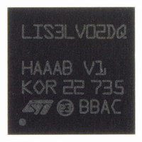
LIS3LV02DQ-TR STMicroelectronics, LIS3LV02DQ-TR Datasheet - Page 4

LIS3LV02DQ-TR
Manufacturer Part Number
LIS3LV02DQ-TR
Description
ACCELEROMETER TRPL AXIS 28QFPN
Manufacturer
STMicroelectronics
Specifications of LIS3LV02DQ-TR
Axis
X, Y, Z
Acceleration Range
±2g, 6g
Sensitivity
1024LSB/g, 340LSB/g
Voltage - Supply
2.16 V ~ 3.6 V
Output Type
Digital
Bandwidth
40Hz ~ 2.56kHz Selectable
Interface
I²C, SPI
Mounting Type
Surface Mount
Package / Case
28-QFN
Sensing Axis
X, Y, Z
Acceleration
2 g, 6 g
Digital Output - Number Of Bits
12 bit, 16 bit
Supply Voltage (max)
3.6 V
Supply Voltage (min)
2.16 V
Supply Current
0.6 mA
Maximum Operating Temperature
+ 85 C
Minimum Operating Temperature
- 40 C
Digital Output - Bus Interface
I2C, SPI
Package Type
QFN
Operating Supply Voltage (min)
2.16V
Operating Supply Voltage (typ)
2.5V
Operating Supply Voltage (max)
3.6V
Operating Temperature (min)
-40C
Operating Temperature (max)
85C
Operating Temperature Classification
Industrial
Product Depth (mm)
7mm
Product Height (mm)
1.75mm
Product Length (mm)
7mm
Mounting
Surface Mount
Pin Count
28
For Use With
497-6249 - BOARD EVAL ACCEL DGTL LIS3LV02DQ497-5069 - EVAL BOARD 3AXIS MEMS ACCELLRMTR
Lead Free Status / RoHS Status
Lead free / RoHS Compliant
Other names
497-6346-2
Available stocks
Company
Part Number
Manufacturer
Quantity
Price
Part Number:
LIS3LV02DQ-TR
Manufacturer:
ST
Quantity:
20 000
LIS3L02DQ
Table 4. Electrical Characteristics
(Temperature range -20°C to +70°C). All the parameters are specified @ Vdd=3.3V and T=25°C unless
otherwise noted.
Notes: 1. Product is factory calibrated at 3.3V.The device can be used from 2.7 V to 3.6 V
3
Stresses above those listed as “absolute maximum ratings” may cause permanent damage to the device.
This is a stress rating only and functional operation of the device under these conditions is not implied.
Exposure to maximum rating conditions for extended periods may affect device reliability.
Table 5. Absolute Maximum Rating
4/20
Symbol
Vdd_IO
IddPdn
Symbol
Vdd_IO
F
A
Vdd
A
BW
Ton
T
DR
ESD
Idd
Vdd
max
Absolute Maximum Rating
Vin
POW
UNP
STG
2. Typical specifications are not guaranteed.
3. Turn on time is related to output rate and it's defined as: Ton =6/DR.Ton time is the time between leaving Power Down mode and
This is an ESD sensitive device, improper handling can cause permanent damages to the part
This is a Mechanical Shock sensitive device, improper handling can cause permanent damages to the part
reaching 99% of actual acceleration value.
Supply Voltage
I/O pads Supply Voltage
Supply Current
Current Consumption in
Power-Down Mode
Digital Filter Cut-Off
frequency (-3dB)
Output Data Rate
SPI Frequency
Turn on time at exit from
Power Down Mode
Supply Voltage
I/O pads Supply Voltage
Input Voltage on any control pin
(CS, SCL/SPC, SDA/SDI/SDO,SDO,RDY/INT)
Acceleration (Any axis, Powered, Vdd=3.3V)
Acceleration (Any axis, Not Powered)
Storage Temperature Range
Electrostatic Discharge Protection
Parameter
3
1
Ratings
T = 25°C
T = 25°C
Dec factor = 128
Dec factor = 64
Dec factor = 32
Dec factor = 8
Dec factor = 128
Dec factor = 64
Dec factor = 32
Dec factor = 8
Vdd_IO<2.4V
Vdd_IO>2.4V
Test Condition
Min.
2.7
1.8
Typ.
6/DR
10000g for 0.1 ms
10000g for 0.1 ms
1120
1120
4480
Maximum Value
140
280
280
560
3000g for 0.5 ms
3000g for 0.5 ms
3.3
-0.3 to Vdd +0.1
-0.3 to Vdd +0.3
70
1
-40 to +125
1.5 (CDM)
200 (MM)
2
1 (HBM)
-0.3 to 6
Vdd+0.1
Max.
3.6
1.5
15
4
8
Unit
MHz
MHz
Unit
kV
kV
°C
mA
ms
µA
Hz
Hz
Hz
Hz
Hz
Hz
Hz
Hz
V
V
V
V
V
V


