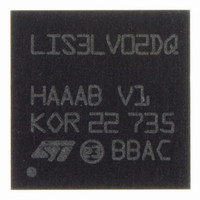
LIS3LV02DQ-TR STMicroelectronics, LIS3LV02DQ-TR Datasheet

LIS3LV02DQ-TR
Specifications of LIS3LV02DQ-TR
Available stocks
Related parts for LIS3LV02DQ-TR
LIS3LV02DQ-TR Summary of contents
Page 1
DIGITAL OUTPUT LINEAR ACCELEROMETER 1 Features ■ 2.7V TO 3.6V SINGLE SUPPLY OPERATION ■ 1.8V COMPATIBLE IOs 12 BIT RESOLUTION ■ 2 ■ I C/SPI DIGITAL OUTPUT INTERFACES ■ INTERRUPT ACTIVATED BY MOTION ■ PROGRAMMABLE INTERRUPT THRESHOLD ...
Page 2
LIS3L02DQ Table 2. Pin Description N° Pin Internally not connected 3 GND 0V supply 4 Vdd Power supply Internally not connected 13 Reserved Leave unconnected or connect to Vdd_IO 14 Reserved Leave ...
Page 3
Table 3. Mechanical Characteristics (Temperature range -20°C to +70°C). All the parameters are specified @ Vdd = 3.3V and T = 25°C unless otherwise noted. Symbol Parameter Ar 3 Acceleration Range So 4 Sensitivity SoDr Sensitivity Change Vs Temperature Off ...
Page 4
LIS3L02DQ Table 4. Electrical Characteristics (Temperature range -20°C to +70°C). All the parameters are specified @ Vdd=3.3V and T=25°C unless otherwise noted. Symbol Parameter Vdd Supply Voltage Vdd_IO I/O pads Supply Voltage Idd Supply Current IddPdn Current Consumption in Power-Down ...
Page 5
Terminology 3.1.1 Sensitivity Sensitivity describes the gain of the sensor and can be determined e.g. by applying 1g acceleration to it. As the sensor can measure DC accelerations this can be done easily by pointing the axis of interest ...
Page 6
LIS3L02DQ 4 Functionality 4.1 Sensing element A proprietary process is utilized to create a surface micro-machined accelerometer. The technology allows to carry out suspended silicon structures which are attached to the substrate in a few points called anchors and are ...
Page 7
Application Hints Figure 4. LIS3L02DQ Electrical Connection 10uF 100nF Vdd GND Digital signal from/to signal controller. Signal’s levels are defined by proper selection of Vdd_IO The device core is supplied through Vdd line (Vdd typ=3.3V) while the I/O pads ...
Page 8
LIS3L02DQ 6 Digital Interfaces The registers embedded inside the LIS3L02DQ may be accessed through both the I terfaces. The latter may be software configured to operate either in SPI mode or in 3-wire interface mode. The serial interfaces are mapped ...
Page 9
The receiver must then pull the data line LOW so that it remains stable low during the HIGH period of the acknowledge clock pulse. A receiver which has been addressed is obliged to generate an acknowledge ...
Page 10
LIS3L02DQ 6.3 SPI Bus Interface The SPI interface present inside the LIS3L02DQ is a bus slave. The SPI allows to write and read the reg- isters of the device. The Serial Interface interacts with the outer world with 4 wires: ...
Page 11
AD(6:0). This is the address field of the indexed register. – bit 8-15: data DO(7:0) (read mode). This is the data that will be read from the device (MSB first). 6.3.3 SPI Write Figure 7. SPI ...
Page 12
LIS3L02DQ 7 Registers mapping The table given below provides a listing of the registers embedded in the device and the related address- es. Table 8. Registers address map Reg. Name Type OFFSET_X rw OFFSET_Y rw OFFSET_Z rw GAIN_X rw GAIN_Y ...
Page 13
Registers Description The device contains a set of registers which are used to control its behavior and to retrieve acceleration data. For normal mode operation it is not necessary to program offset and gain code as they are loaded ...
Page 14
LIS3L02DQ 8.7 CTRL_REG1 (20h) Control Register 1 and 2 allow to influence the signal chain and start up conditions as well as the commu- nication setup. PD1 PD1, PD0 Power Down Control. Default value: 00 (00: power-down mode; x1,1x: normal ...
Page 15
WAKE_UP_CFG (23h) AOI AOI And/Or combination of Interrupt events. Default value: 0 (0: OR combination of interrupt events; 1: AND combination of interrupt events) LIR Latch interrupt request into WAKE_UP_SOURCE reg with the WAKE_UP_SOURCE reg cleared by reading WAKE_UP_ACK ...
Page 16
LIS3L02DQ 8.11 WAKE_UP_ACK (25h) Reading at this address resets the WAKE_UP_SOURCE register. 8.12 A_STATUS_REG (27h) ZYXOR ZYXOR X, Y and Z axis Data Overrun ZOR Z axis Data Overrun YOR Y axis Data Overrun XOR X axis Data Overrun ZYXDA ...
Page 17
OUTY_H (2Bh) When reading the register in “12 bit right justified” mode the most significant bits (7:4) are replaced with bit 3 (i.e. YD15- . YD12=YD11, YD11, YD11, YD11) YD15 YD14 YD15, YD8 Y axis acceleration data MSB 8.17 ...
Page 18
LIS3L02DQ 9 Package Information Figure 9. QFN-44 Mechanical Data & Package Dimensions mm DIM. MIN. TYP. MAX. A 1.70 1.80 1.90 A1 0.19 0.21 b 0.20 0.25 0.30 D 7.0 E 7.0 e 0.50 J 5.04 5.24 K 5.04 5.24 ...
Page 19
Revision History Table 9. Revision History Date Revision February 2004 January 2005 20 January, 2005 May 2005 1 First Issue 2 Changed the Operating Temperature range: from -40°C to +85°C to -20°C to +70°C. Changed some data on the ...
Page 20
... No license is granted by implication or otherwise under any patent or patent rights of STMicroelectronics. Specifications mentioned in this publication are subject to change without notice. This publication supersedes and replaces all information previously supplied. STMicroelectronics products are not authorized for use as critical components in life support devices or systems without express written approval of STMicroelectronics ...


