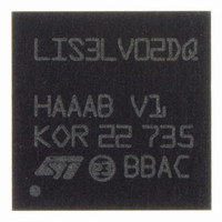
LIS3LV02DQ-TR STMicroelectronics, LIS3LV02DQ-TR Datasheet - Page 10

LIS3LV02DQ-TR
Manufacturer Part Number
LIS3LV02DQ-TR
Description
ACCELEROMETER TRPL AXIS 28QFPN
Manufacturer
STMicroelectronics
Specifications of LIS3LV02DQ-TR
Axis
X, Y, Z
Acceleration Range
±2g, 6g
Sensitivity
1024LSB/g, 340LSB/g
Voltage - Supply
2.16 V ~ 3.6 V
Output Type
Digital
Bandwidth
40Hz ~ 2.56kHz Selectable
Interface
I²C, SPI
Mounting Type
Surface Mount
Package / Case
28-QFN
Sensing Axis
X, Y, Z
Acceleration
2 g, 6 g
Digital Output - Number Of Bits
12 bit, 16 bit
Supply Voltage (max)
3.6 V
Supply Voltage (min)
2.16 V
Supply Current
0.6 mA
Maximum Operating Temperature
+ 85 C
Minimum Operating Temperature
- 40 C
Digital Output - Bus Interface
I2C, SPI
Package Type
QFN
Operating Supply Voltage (min)
2.16V
Operating Supply Voltage (typ)
2.5V
Operating Supply Voltage (max)
3.6V
Operating Temperature (min)
-40C
Operating Temperature (max)
85C
Operating Temperature Classification
Industrial
Product Depth (mm)
7mm
Product Height (mm)
1.75mm
Product Length (mm)
7mm
Mounting
Surface Mount
Pin Count
28
For Use With
497-6249 - BOARD EVAL ACCEL DGTL LIS3LV02DQ497-5069 - EVAL BOARD 3AXIS MEMS ACCELLRMTR
Lead Free Status / RoHS Status
Lead free / RoHS Compliant
Other names
497-6346-2
Available stocks
Company
Part Number
Manufacturer
Quantity
Price
Part Number:
LIS3LV02DQ-TR
Manufacturer:
ST
Quantity:
20 000
LIS3L02DQ
6.3 SPI Bus Interface
The SPI interface present inside the LIS3L02DQ is a bus slave. The SPI allows to write and read the reg-
isters of the device. The Serial Interface interacts with the outer world with 4 wires: CS, SPC, SDI and
SDO.The maximum frequency is related to the Vdd_IO supply voltage.In particular in the 2.4 V - 3.6 V
range is 8 MHz while under 2.4 V is 4 MHz.
6.3.1 Read & Write registers
Figure 5. Read & write protocol
CS is the Serial Port Enable and it is controlled by the SPI master. It goes low at the start of the transmis-
sion and goes back high at the end. SPC is the Serial Port Clock and it is controlled by the SPI master. It
is stopped high when CS is high (no transmission). SDI and SDO are respectively the Serial Port Data
Input and Output. Those lines are driven at the falling edge of SPC and should be captured at the rising
edge of SPC.
Both the Read Register and Write Register commands are completed in 16 clock pulses. Bit duration is
the time between two falling edges of SPC. The first bit (bit 0) starts at the first falling edge of SPC after
the falling edge of CS while the last bit (bit 15) starts at the last falling edge of SPC just before the rising
edge of CS.
6.3.2 SPI Read
Figure 6. SPI Read protocol
The SPI Read command consists of 16 clock pulses:
10/20
– bit 0: RW bit. When 0, the data DI(7:0) is written into the device. When 1, the data DO(7:0) from the
– bit 1-7: address AD(6:0). This is the address field of the indexed register.
– bit 8-15: data DI(7:0) (write mode). This is the data that will be written into the device (MSB first).
– bit 8-15: data DO(7:0) (read mode). This is the data that will be read from the device (MSB first).
– bit 0: READ bit. The value is 1.
device is read. In latter case, the chip will drive SDO at the start of bit 8.
SPDO
SPC
SDI
SPDO
CS
SPDI
SPC
CS
RW
RW
AD6 AD5 AD4 AD3 AD2 AD1 AD0
AD6 AD5 AD4 AD3 AD2 AD1 AD0
DO7 DO6 DO5 DO4 DO3 DO2 DO1 DO0
DO7 DO6 DO5 DO4 DO3 DO2 DO1 DO0
DI7 DI6 DI5 DI4 DI3 DI2 DI1 DI0


