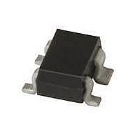
BFU630F,115 NXP Semiconductors, BFU630F,115 Datasheet - Page 2

BFU630F,115
Manufacturer Part Number
BFU630F,115
Description
TRANSISTOR NPN SOT343F
Manufacturer
NXP Semiconductors
Datasheet
1.BFU630F115.pdf
(12 pages)
Specifications of BFU630F,115
Transistor Type
NPN
Voltage - Collector Emitter Breakdown (max)
5.5V
Frequency - Transition
21GHz
Noise Figure (db Typ @ F)
0.75dB ~ 1.3dB @ 1.5GHz ~ 5.8GHz
Gain
13dB ~ 22.5dB
Power - Max
200mW
Dc Current Gain (hfe) (min) @ Ic, Vce
90 @ 5mA, 2V
Current - Collector (ic) (max)
30mA
Mounting Type
Surface Mount
Package / Case
SOT-343F
Configuration
Single
Transistor Polarity
NPN
Collector- Emitter Voltage Vceo Max
5.5 V
Emitter- Base Voltage Vebo
2.5 V
Continuous Collector Current
3 mA
Power Dissipation
200 mW
Maximum Operating Temperature
+ 150 C
Dc Collector/base Gain Hfe Min
90
Gain Bandwidth Product Ft
21 GHz
Mounting Style
SMD/SMT
Lead Free Status / RoHS Status
Lead free / RoHS Compliant
NXP Semiconductors
2. Pinning information
3. Ordering information
BFU630F
Product data sheet
1.4 Quick reference data
Table 1.
[1]
[2]
Table 2.
Table 3.
Symbol Parameter
V
V
V
I
P
h
C
NF
P
Pin
1
2
3
4
Type number
f
G
BFU630F
C
T
FE
CBO
CEO
EBO
tot
L(1dB)
CBS
p(max)
T
G
sp
p(max)
is the temperature at the solder point of the emitter lead.
collector-base voltage
collector-emitter voltage
emitter-base voltage
collector current
total power dissipation
DC current gain
collector-base
capacitance
transition frequency
maximum power gain
noise figure
output power at 1 dB
gain compression
is the maximum power gain, if K > 1. If K < 1 then G
Quick reference data
Discrete pinning
Ordering information
emitter
base
emitter
collector
Description
All information provided in this document is subject to legal disclaimers.
Package
Name
-
Rev. 1 — 15 December 2010
Description
plastic surface-mounted flat pack package; reverse
pinning; 4 leads
Conditions
open emitter
open base
open collector
T
I
T
V
I
f = 2 GHz; T
I
f = 2.4 GHz; T
I
f = 2.4 GHz;
I
Z
f = 2.4 GHz; T
C
C
C
C
C
sp
j
S
CB
= 5 mA; V
= 25 C
= 10 mA; V
= 15 mA; V
= 3 mA; V
= 30 mA; V
= Z
90 C
= 2 V; f = 1 MHz
L
= 50 ;
amb
CE
CE
CE
CE
CE
amb
S
amb
= 2 V;
= 2 V;
=
= 25 C
= 2 V;
= 2 V;
= 2.5 V;
Simplified outline
= 25 C
= 25 C
opt
NPN wideband silicon RF transistor
p(max)
3
2
= Maximum Stable Gain (MSG).
[1]
[2]
1
4
Min
-
-
-
-
-
90
-
-
-
-
-
Typ
-
-
-
3
-
135
47
21
24.5
0.85
11.5
Graphic symbol
BFU630F
© NXP B.V. 2010. All rights reserved.
2
16
Max
5.5
2.5
30
200
180
-
-
-
-
-
mbb159
Version
SOT343F
1, 3
4
Unit
V
V
V
mA
mW
fF
GHz
dB
dB
dBm
2 of 12


