BFU630F,115 NXP Semiconductors, BFU630F,115 Datasheet
BFU630F,115
Specifications of BFU630F,115


Related parts for BFU630F,115


BFU630F,115 Summary of contents
Page 1
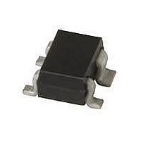
BFU630F NPN wideband silicon RF transistor Rev. 1 — 15 December 2010 1. Product profile 1.1 General description NPN silicon microwave transistor for high speed, low noise applications in a plastic, 4-pin dual-emitter SOT343F package. CAUTION This device is sensitive ...
Page 2
... NXP Semiconductors 1.4 Quick reference data Table 1. Symbol Parameter V CBO V CEO V EBO tot CBS p(max L(1dB) [ the temperature at the solder point of the emitter lead. sp [2] G p(max) 2. Pinning information Table 2. Pin Ordering information Table 3. Type number BFU630F BFU630F Product data sheet Quick reference data ...
Page 3
... NXP Semiconductors 4. Marking Table 4. Type number BFU630F 5. Limiting values Table 5. In accordance with the Absolute Maximum Rating System (IEC 60134). Symbol V CBO V CEO V EBO tot T stg the temperature at the solder point of the emitter lead Thermal characteristics Table 6. Symbol R th(j-sp) Fig 1. ...
Page 4
... NXP Semiconductors 7. Characteristics Table 7. Characteristics unless otherwise specified j Symbol Parameter V collector-base breakdown voltage (BR)CBO V collector-emitter breakdown voltage (BR)CEO I collector current C I collector-base cut-off current CBO h DC current gain FE C collector-emitter capacitance CES C emitter-base capacitance EBS C collector-base capacitance CBS f transition frequency ...
Page 5
... NXP Semiconductors Table 7. Characteristics …continued unless otherwise specified j Symbol Parameter IP3 third-order intercept point [ the maximum power gain > < 1 then G p(max (2) (mA) (3) 20 (4) (5) 15 (6) (7) 10 (8) (9) 5 (10 C. T amb = 200 A ( 180 A ( 160 A ( 140 A ( 120 A ...
Page 6
... NXP Semiconductors 80 C CBS (fF MHz, T amb Fig 4. Collector-base capacitance as a function of collector-base voltage; typical values = 25 amb ( 1.5 GHz ( 1.8 GHz ( 2.4 GHz ( 5.8 GHz Fig 6. Gain as a function of collector current; typical value BFU630F Product data sheet 001aam815 fT (GHz (V) CB Fig 5 ...
Page 7
... NXP Semiconductors 50 G (dB MSG 20 G p(max) 2 |S21 mA amb Fig 7. Gain as a function of frequency; typical values 2.0 NF min (dB) 1.6 1.2 0.8 0 amb ( 5.8 GHz ( 2.4 GHz ( 1.8 GHz ( 1.5 GHz Fig 9. Minimum noise figure as a function of collector current; typical values BFU630F ...
Page 8
... NXP Semiconductors 8. Package outline Plastic surface-mounted flat pack package; reverse pinning; 4 leads DIMENSIONS (mm are the original dimensions) A UNIT max 0.75 0.4 0.7 0.25 mm 0.65 0.3 0.5 0.10 OUTLINE VERSION IEC SOT343F Fig 11. Package outline SOT343F BFU630F Product data sheet scale 2.2 1 ...
Page 9
... NXP Semiconductors 9. Abbreviations Table 8. Acronym AMR CDMA DC DRO FM GPS LNA LNB LTE NPN RF RKE UMTS WLAN 10. Revision history Table 9. Revision history Document ID Release date BFU630F v.1 20101215 BFU630F Product data sheet Abbreviations Description Automatic Meter Reading Code Division Multiple Access Direct Current ...
Page 10
... In no event shall NXP Semiconductors be liable for any indirect, incidental, punitive, special or consequential damages (including - without limitation - lost profits, lost savings, business interruption, costs related to the removal or ...
Page 11
... NXP Semiconductors’ specifications such use shall be solely at customer’s own risk, and (c) customer fully indemnifies NXP Semiconductors for any 12. Contact information For more information, please visit: ...
Page 12
... NXP Semiconductors 13. Contents 1 Product profile . . . . . . . . . . . . . . . . . . . . . . . . . . 1 1.1 General description . . . . . . . . . . . . . . . . . . . . . 1 1.2 Features and benefits . . . . . . . . . . . . . . . . . . . . 1 1.3 Applications . . . . . . . . . . . . . . . . . . . . . . . . . . . 1 1.4 Quick reference data . . . . . . . . . . . . . . . . . . . . 2 2 Pinning information . . . . . . . . . . . . . . . . . . . . . . 2 3 Ordering information . . . . . . . . . . . . . . . . . . . . . 2 4 Marking . . . . . . . . . . . . . . . . . . . . . . . . . . . . . . . . 3 5 Limiting values Thermal characteristics . . . . . . . . . . . . . . . . . . 3 7 Characteristics . . . . . . . . . . . . . . . . . . . . . . . . . . 4 8 Package outline . . . . . . . . . . . . . . . . . . . . . . . . . 8 9 Abbreviations . . . . . . . . . . . . . . . . . . . . . . . . . . . 9 10 Revision history . . . . . . . . . . . . . . . . . . . . . . . . . 9 11 Legal information ...