EVAL-PAN1321 Panasonic, EVAL-PAN1321 Datasheet - Page 41
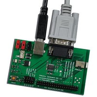
EVAL-PAN1321
Manufacturer Part Number
EVAL-PAN1321
Description
Bluetooth / 802.15.1 Modules & Development Tools
Manufacturer
Panasonic
Specifications of EVAL-PAN1321
Wireless Frequency
2.4 GHz
Interface Type
I2C, JTAG, UART
Data Rate
3 Mbps
Modulation
DQPSK
Operating Voltage
2.7 V to 3.6 V
Operating Temperature Range
- 40 C to + 85 C
Output Power
2.5 dBm
Technology/ Type
PAN1321 Evaluation Kit
Processor Series
PAN1321
For Use With/related Products
ENW-89811K4CF
Lead Free Status / RoHS Status
Lead free / RoHS Compliant


9.9
9.9.1
The content of voids is larger on LGA modules than for modules with BGA or leads. At a LGA solder joint the
outgassing flux has a longer way to the surface of the solder and it has a relatively small surface to the air.
The void content of the PAN1321 module conforms to IPC-A-610D (25% or less voiding area/area).
Figure 17
whole spectra of void content variation within the same lot and occasion of assembly.
Figure 17
9.9.2
If the void content has to be reduced following parameters have an impact.
Solderability on module and PCB
Bad solderability is often connected to oxidation and has therefore a major impact on voiding. Flux will get
entrapped on oxidized surfaces. In general, Ni/Au pads show fewer voids than HASL and OSP.
Solder paste
Higher activity of the flux will remove oxide rapidly and less flux will get entrapped.
Voiding increases with increasing solder paste exposure time, since long exposure time will result in more
oxidation and moisture pickup.
Pad size
A large soldering pad means that the outgassing flux has a longer way to the surface of the solder, and will thereby
create more voids.
Solder paste
Smaller powder size and higher metal load means more metal surface to deoxidize and thereby more entrapped
flux and voiding. Higher metal load does also mean higher viscosity and more difficult for outgassed flux to remove
from the solder.
Hardware Description
User’s Manual
shows an example of void-content at a module assembled at production site. Normally you can see the
Voids in the Solder Joints
Expected Void Content and Reliability
X-ray Picture Showing Voids Conforming to IPC-A-610D
Parameters with an Impact on Voiding
41
V oids _I P C _A _ 610D .v s d
Revision 3.1, 2011-01-18
Assembly Guidelines
ENW89811K4CF
PAN1321-SPP
Related parts for EVAL-PAN1321
Image
Part Number
Description
Manufacturer
Datasheet
Request
R

Part Number:
Description:
ENERCHIP CC EVAL KIT
Manufacturer:
Cymbet Corporation
Datasheet:

Part Number:
Description:
BOARD EVAL FOR AD976
Manufacturer:
Analog Devices Inc
Datasheet:

Part Number:
Description:
BOARD EVAL FOR ADXL345
Manufacturer:
Analog Devices Inc
Datasheet:

Part Number:
Description:
ENERCHIP CC SEH EVAL KIT
Manufacturer:
Cymbet Corporation
Datasheet:

Part Number:
Description:
ENERCHIP EP ENERGY HARVEST EVAL
Manufacturer:
Cymbet Corporation
Datasheet:

Part Number:
Description:
EVAL BOARD FOR TW6864-LB2-GR
Manufacturer:
Intersil
Datasheet:
Part Number:
Description:
EVAL BOARD FOR TW8816-LB3-GR
Manufacturer:
Intersil
Datasheet:
Part Number:
Description:
EVAL BOARD FOR TW8817-TA3-GRS
Manufacturer:
Intersil
Datasheet:

Part Number:
Description:
EVALUATION MODULE FOR ADUM4160
Manufacturer:
Analog Devices Inc
Datasheet:

Part Number:
Description:
BOARD EVALUATION ADCMP581BCP
Manufacturer:
Analog Devices Inc
Datasheet:
Part Number:
Description:
BOARD EVALUATION ADM1041
Manufacturer:
Analog Devices Inc
Datasheet:

Part Number:
Description:
EVAL BOARD FOR STM32F107VCT
Manufacturer:
STMicroelectronics
Datasheet:
Part Number:
Description:
BOARD EVAL FOR AD1954
Manufacturer:
Analog Devices Inc
Datasheet:
Part Number:
Description:
BOARD EVAL FOR AD1955
Manufacturer:
Analog Devices Inc
Datasheet:

Part Number:
Description:
BOARD EVAL FOR AD7655
Manufacturer:
Analog Devices Inc
Datasheet: