EVAL-PAN1321 Panasonic, EVAL-PAN1321 Datasheet
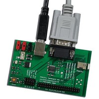
EVAL-PAN1321
Specifications of EVAL-PAN1321


Related parts for EVAL-PAN1321


EVAL-PAN1321 Summary of contents
Page 1
...
Page 2
... Panasonic Office. Panasonic Electronic Devices may only be used in life-support devices or systems with the express written approval of Panasonic Devices failure of such components can reasonably be expected to cause the failure of that life-support device or system affect the safety or effectiveness of that device or system. Life support devices or systems are intended to be implanted in the human body support and/or maintain and sustain and/or protect human life ...
Page 3
... Studio™, SSI™ of Texas Instruments Incorporated. Bluetooth Association. Java™, SunOS™, Solaris™ of Sun Microsystems, Inc. Philips ® Electronics N.V. Epson of Seiko Epson Corporation. Seiko ® Panasonic of Matsushita Electric Industrial Co., Ltd. Murata of Taiyo Yuden Co., Ltd. TDK ® Semiconductor , MICROWIRE™ of National Semiconductor Corporation. IEEE Electronics Engineers, Inc ...
Page 4
Table of Contents Table of Contents . . . . . . . . . . . . . . . . . . . . . . . . . . . . . . . . . . ...
Page 5
Package Information . . . . . . . . . . . . . . . . . . . . . . . . . . . . . . . . . . . . . ...
Page 6
List of Figures Figure 1 Simplified Block Diagram of PAN1321-SPP . . . . . . . . . . . . . . . . . . . . . . . . . . . . . . ...
Page 7
List of Tables Table 1 Pin Description . . . . . . . . . . . . . . . . . . . . . . . . . . . . . . . . . ...
Page 8
General Device Overview 1.1 Features General • Complete Bluetooth 2.0 + EDR solution – Configurable for BT 1.2 Ultra low power design in 0.13 μm CMOS • • Temperature range from -40°C to 85°C • Integrates ARM7TDMI, RAM and ...
Page 9
Block Diagram PAN1321-SPP VDD1 VDD_UART UART GPIO V Voltage supply Regulator Figure 1 Simplified Block Diagram of PAN1321-SPP 1.3 Pin Configuration LGA 1.0 0 ...
Page 10
Pin Description The non-shaded cells indicate pins that will be fixed for the product lifetime. Shaded cells indicate that the pin might be removed/changed in future variants. Pins not listed below shall not be connected. Table 1 Pin Description ...
Page 11
Table 1 Pin Description Pin Symbol Input / No. Output F4 P0.14 I/O F5 P0.7 / I/O/OD UARTCTS F7 P0.4 / I/O/OD UARTTXD F8 P0.6 / I/O/OD UARTRTS A4, VSUPPLY SI A5 VREG SO F6 VDDUART SI C5 ...
Page 12
System Integration PAN1321-SPP is optimized for a low bill of material (BOM) and a small PCB size. application example. Keys, Leds GPIO Oscillator I EEPROM Voltage Regulator VSUPPLY Figure 3 Example of a Bluetooth System using eUniStone User’s Manual ...
Page 13
The UART interface is used for communication between the host and PAN1321-SPP. The lines UARTTXD and UARTRXD are used for commands, events and data. The lines UARTRTS and UARTCTS are used for hardware flow control. Low power mode control of ...
Page 14
Basic Operating Information 2.1 Power Supply PAN1321-SPP is supplied from a single supply voltage VSUPPLY. This supply voltage must always be present. The PAN1321-SPP chip is supplied from an internally generated 2.5 V supply voltage. This voltage can be ...
Page 15
Interfaces 3.1 UART Interface The UART interface is the main communication interface between the host and PAN1321-SPP. The interface consists of four UART signals and two wake-up signals as shown in Host UARTTXD UARTRXD UARTRTS UARTCTS WAKEUP_BT WAKEUP_HOST Figure ...
Page 16
General Device Capabilities This chapter describes features available in the PAN1321 (ENW89811K4CF 22/xx) core. Actual feature set and how to access the features can be found in the AT Command document [1]. Release specific performance characteristics, like data speed, ...
Page 17
Bluetooth Capabilities 5.1 Supported Features • Bluetooth V2.0 + EDR compliant • Enhanced Data Rate Mbit/s • Adaptive Frequency Hopping (AFH) • All packet types • Authentication, Pairing and Encryption • SPP Device A and B ...
Page 18
PAN1321-SPP Specifics and Extensions 5.2.1 During Connection 5.2.1.1 Role Switch Only one role switch can be performed at a time role switch request is pending, other role switch requests on the same or other links are rejected. ...
Page 19
RSSI and Output Power Control 5.2.2.1 Received Signal Strength Indication (RSSI) PAN1321-SPP supports received signal strength measurements and uses LMP signaling to keep the output power of a remote device within the golden receive power range. The range is ...
Page 20
Electrical Characteristics 6.1 Absolute Maximum Ratings Table 3 Absolute Maximum Ratings Parameter Symbol Storage temperature VSUPPLY supply voltage VDDUART supply voltage VDD1 supply voltage VREG VREG ONOFF Input voltage range Output voltage range ESD Note: Stresses above those listed ...
Page 21
DC Characteristics 6.3.1 Pad Driver and Input Stages For more information, see Chapter Table 5 Internal1 (1.5 V) Supplied Pins Parameter Input low voltage Input high voltage Output low voltage Output high voltage 1) Continuous Load Pin Capacitance Magnitude ...
Page 22
Table 7 VDDUART Supplied Pins (cont’d) Parameter Symbol Output low voltage Output low voltage Output high voltage Output high voltage 1) Continuous Load Pin Capacitance Magnitude Pin Leakage 1) The totaled continuous load for all VDDUART supplied pins shall not ...
Page 23
Pull-ups and Pull-downs Table 10 Pull-up and Pull-down Currents Pin Min. P0.12 260 P0.13 P0.0 22 P0.1 P0.2 P0.3 P0.4 4.2 P0.5 P0.6 P0.7 P0.10 P0.8 P0.9 P0.11 P0.14 P0.15 P1.0 1.1 P1.1 P1.2 P1.3 P1.4 P1.5 P1.6 P1.7 ...
Page 24
System Power Consumption Table 11 Max. Load at the Different Supply Voltages Parameter Vsupply Note: I/O currents are not included since they depend mainly on external loads. 6.4 AC Characteristics 6.5 RF Part 6.5.1 Characteristics RF Part The characteristics ...
Page 25
Table 12 BDR - Transmitter Part (cont’d) Parameter Symbol Carrier frequency drift (one slot) |fdrift| Carrier frequency drift (three slots) |fdrift| Carrier frequency drift (five slots) |fdrift| Carrier frequency driftrate (one slot) |fdriftrate| Carrier frequency driftrate (three slots) |fdriftrate| Carrier ...
Page 26
Table 13 BDR -Receiver Part (cont’d) Parameter Symbol Intermodulation performance Maximum input level Table 14 EDR - Transmitter Part Parameter Output power (high gain) Relative transmit power: PxPSK - PGFSK Carrier frequency stability |ωi| Carrier frequency stability |ωi+ω0| Carrier frequency ...
Page 27
Table 15 EDR -Receiver Part (cont’d) Parameter DQPSK - C/I-performance: -1st adjacent channel DQPSK - C/I-performance: co. channel DQPSK - C/I-performance: +1st adjacent channel DQPSK - C/I-performance: +2nd adjacent channel DQPSK - C/I-performance: +3rd adjacent channel 8DPSK - C/I-performance: -4th ...
Page 28
... Tolerances on all outer dimensions, height, width and length, are +/- 0.2 mm. User’s Manual Hardware Description HW/SW PCB Case 28 PAN1321-SPP ENW89811K4CF Package Information Version HW – Hardware Version SW – Software Version Machine readable 2D bar code Panasonic usage only, could be changed without any notice Production _Package.vsd Revision 3.1, 2011-01-18 ...
Page 29
Pin Mark Pin 1 (A1) is marked on bottom footprint and on the top of the shield on the module according to Diameter of pin 1 mark on the shield is 0.15 mm. PAN1321 22/07 ENW89811K4CF 0902401 FCC ID:T7VEBMU ...
Page 30
Important Application Information 8.1 Reference Design Figure 8 Reference Design Schematics User’s Manual Hardware Description Important Application Information 30 Revision 3.1, 2011-01-18 PAN1321-SPP ENW89811K4CF ...
Page 31
ENW89811K4CF 22/xx is intended to be installed inside end user equipment. ENW89811K4CF 22/xx is Bluetoooth-qualified and also FCC-certified and Industry Canada approved, and conforms to R&TTE (European) requirements and directives with the reference design described in with the following antennas, ...
Page 32
... European R&TTE Declaration of Conformity Hereby, Panasonic Electronic Devices Europe GmbH, declares that the Bluetooth module ENW89811K4CF 22/ compliance with the essential requirements and other relevant provisions of Directive 1999/5/EC result of the conformity assessment procedure described in Annex III of the Directive 1999/5/EC, the end- ...
Page 33
... IEC 60950-1 (2006 301 489-1 V1.8 301 489-17 V2.1 300 328 V1.6.1 (2004-11 300 328 V1.7.1 (2006-10) The technical contruction file is kept available at: Panasonic Electronic Devices Europe GmbH, Zeppelinstrasse 19, 21337 Lueneburg, Germany Issued on: Signed by the manufacturer: (Company name) (Signature) (Printed name) ...
Page 34
... It is recommended to include the following information on the host product label: Contains transmitter Module FCC ID: T7VEBMU / IC: 216QEBMU 8.10 Regulatory Test House The test house used by Panasonic in the Bluetooth and Regulatory approvals for the module PAN1321: Eurofins Product Service GmbH Storkower Str. 38c D-15526 Reichenwalde b. Berlin GERMANY Tel ...
Page 35
Assembly Guidelines The target of this document is to provide guidelines for customers to successfully introduce the PAN1321-SPP module in production. This includes general description, PCB-design, solder printing process, assembly, soldering process, rework and inspection. 9.1 General Description of ...
Page 36
... This means that the PAN1321 module can be assembled with a variety of placement systems recommended to use a vision system capable of package pad recognition and alignment that evaluates the pad locations on the package (in contrast to outline centring). This eliminates the pad to package edge tolerance. ...
Page 37
Package PAN1321 is packed in tape on reel according to Figure 13 Tape on Reel User’s Manual Hardware Description Figure 13. 37 PAN1321-SPP ENW89811K4CF Assembly Guidelines Revision 3.1, 2011-01-18 ...
Page 38
Soldering Profile Generally all standard reflow soldering processes (vapour phase, convection, infrared) and typical temperature profiles used for surface mount devices are suitable for the PAN1321 module. Wave soldering is not possible. Figure 14 and Figure 15 shows example ...
Page 39
At the reflow process each solder joint has to be exposed to temperatures above solder liquids for a sufficient time to get the optimum solder joint quality, whereas overheating the board with its components has to be avoided. Using infrared ...
Page 40
Alternative 2: Printing Solder To print solder on the module a fixture must be used. The purpose of the fixture is to get a flat surface and fix the stencil and module for printing. An example of how this ...
Page 41
... Expected Void Content and Reliability The content of voids is larger on LGA modules than for modules with BGA or leads LGA solder joint the outgassing flux has a longer way to the surface of the solder and it has a relatively small surface to the air. The void content of the PAN1321 module conforms to IPC-A-610D (25% or less voiding area/area). ...
Page 42
Stencil thickness A thick solder paste stencil means more surface area to the air and thereby easier for the outgassing flux to leave the solder. Temperature soldering profile Too short preheat time means that the flux does not get enough ...
Page 43
Terminology A ACK Acknowledgement ARQ Automatic Repeat reQuest B b bit/bits (e.g. kb/s) B Byte/Bytes (e.g. kB/s) BALUN BALanced UNbalanced BD_ADDR Bluetooth Device Address BER Bit Error Rate BMU BlueMoon Universal BOM Bill Of Material BT Bluetooth BW Bandwidth C ...
Page 44
Extended Synchronous Connection-Oriented (logical transport) EV Extended Voice (packet type) F FEC Forward Error Correction FHS Frequency Hop Synchronization (packet) FIFO First In First Out (buffer) FM Frequency Modulation FW Firmware G GFSK Gaussian Frequency Shift Keying (modulation) GPIO ...
Page 45
MSB Most Significant Bit/Byte MSRS Master-Slave Role Switch Connection NOP No OPeration NVM Non-Volatile Memory O OCF Opcode Command Field OGF Opcode Group Field P PA Power Amplifier PCB Printed Circuit Board PCM Pulse Coded Modulation PDU ...
Page 46
TDI Test Data In (JTAG signal) TDO Test Data Out (JTAG signal) TL Transport Layer TMS Test Mode Select (JTAG signal) TX Transmit TXD Transmit Data (UART signal) U UART Universal Asynchronous Receiver & Transmitter ULPM Ultra Low Power Mode ...
Page 47
References [1] SPP-AT Application on PAN1311; Software Version 1.1; Release Notes; Rev3.0 (PAN1311_SPP_AT_V10.03_V1.1_RN_Rev3.0.pdf) [2] SPP-AT User's Manual Software Description ; Rev3.0 (PAN1311_SPP_AT_V10.03_V1.1_UM_SD_Rev3.0.pdf) User’s Manual Hardware Description 47 Revision 3.1, 2011-01-18 PAN1321-SPP ENW89811K4CF References ...
Page 48
... Published by Panasonic Electronic Devices Europe GmbH ...