EVAL-PAN1321 Panasonic, EVAL-PAN1321 Datasheet - Page 40
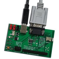
EVAL-PAN1321
Manufacturer Part Number
EVAL-PAN1321
Description
Bluetooth / 802.15.1 Modules & Development Tools
Manufacturer
Panasonic
Specifications of EVAL-PAN1321
Wireless Frequency
2.4 GHz
Interface Type
I2C, JTAG, UART
Data Rate
3 Mbps
Modulation
DQPSK
Operating Voltage
2.7 V to 3.6 V
Operating Temperature Range
- 40 C to + 85 C
Output Power
2.5 dBm
Technology/ Type
PAN1321 Evaluation Kit
Processor Series
PAN1321
For Use With/related Products
ENW-89811K4CF
Lead Free Status / RoHS Status
Lead free / RoHS Compliant


9.6.2.2
To print solder on the module a fixture must be used. The purpose of the fixture is to get a flat surface and fix the
stencil and module for printing. An example of how this fixture can be designed is shown in
Figure 16
1. Assemble the fixture to the bottom
2. Place the module in the cavity with the LGA pads upwards
3. Place the solder paste stencil on the fixture and make sure it fits to the tooling pins and the module
4. Apply vacuum to fix the solder paste stencil
5. Apply solder paste on the stencil and print by using a blade
6. Turn everything (bottom, fixture and stencil) upside down.
7. Separate carefully the bottom from the fixture
8. Pick the module by a nozzle and place in the right position on the board
9. Reflow the solder.
9.7
Automatic inspection of the solder paste printing before assembly is highly recommended to ensure high yield and
good long term reliability.
9.8
If it is intended to send a defect PAN1321 module back to the supplier for failure analysis, please note that during
the removal of this component no further defects must be introduced to the device, because this may hinder the
failure analysis at the supplier. This includes ESD precautions, not to apply high mechanical force for component
removal, and to prevent excess moisture content in the package during salvage (risk of pop corning failures).
Therefore if the maximum storage time out of the dry pack (see label on packing material) is exceeded after board
assembly, the PCB has to be dried 24h at 125°C before soldering off the defect component, because otherwise
too much moisture may have been accumulated.
Hardware Description
User’s Manual
Alternative 2: Printing Solder
Solder Printing
Inspection
Component Salvage
Vacuum hol es
C avity of the module
S older paste stencil
B ottom
40
T ooling pins
S older _P rint ing . v s d
Fixture
Revision 3.1, 2011-01-18
Assembly Guidelines
ENW89811K4CF
Figure
PAN1321-SPP
16.
Related parts for EVAL-PAN1321
Image
Part Number
Description
Manufacturer
Datasheet
Request
R

Part Number:
Description:
ENERCHIP CC EVAL KIT
Manufacturer:
Cymbet Corporation
Datasheet:

Part Number:
Description:
BOARD EVAL FOR AD976
Manufacturer:
Analog Devices Inc
Datasheet:

Part Number:
Description:
BOARD EVAL FOR ADXL345
Manufacturer:
Analog Devices Inc
Datasheet:

Part Number:
Description:
ENERCHIP CC SEH EVAL KIT
Manufacturer:
Cymbet Corporation
Datasheet:

Part Number:
Description:
ENERCHIP EP ENERGY HARVEST EVAL
Manufacturer:
Cymbet Corporation
Datasheet:

Part Number:
Description:
EVAL BOARD FOR TW6864-LB2-GR
Manufacturer:
Intersil
Datasheet:
Part Number:
Description:
EVAL BOARD FOR TW8816-LB3-GR
Manufacturer:
Intersil
Datasheet:
Part Number:
Description:
EVAL BOARD FOR TW8817-TA3-GRS
Manufacturer:
Intersil
Datasheet:

Part Number:
Description:
EVALUATION MODULE FOR ADUM4160
Manufacturer:
Analog Devices Inc
Datasheet:

Part Number:
Description:
BOARD EVALUATION ADCMP581BCP
Manufacturer:
Analog Devices Inc
Datasheet:
Part Number:
Description:
BOARD EVALUATION ADM1041
Manufacturer:
Analog Devices Inc
Datasheet:

Part Number:
Description:
EVAL BOARD FOR STM32F107VCT
Manufacturer:
STMicroelectronics
Datasheet:
Part Number:
Description:
BOARD EVAL FOR AD1954
Manufacturer:
Analog Devices Inc
Datasheet:
Part Number:
Description:
BOARD EVAL FOR AD1955
Manufacturer:
Analog Devices Inc
Datasheet:

Part Number:
Description:
BOARD EVAL FOR AD7655
Manufacturer:
Analog Devices Inc
Datasheet: