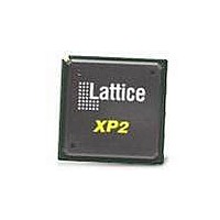
LFXP2-8E-7FT256C Lattice, LFXP2-8E-7FT256C Datasheet - Page 323

LFXP2-8E-7FT256C
Manufacturer Part Number
LFXP2-8E-7FT256C
Description
FPGA - Field Programmable Gate Array 8K LUTs 201I/O Inst- on DSP 1.2V -7 Spd
Manufacturer
Lattice
Datasheet
1.LFXP2-8E-5FTN256I.pdf
(341 pages)
Specifications of LFXP2-8E-7FT256C
Number Of Macrocells
8000
Number Of Programmable I/os
201
Data Ram Size
226304
Supply Voltage (max)
1.26 V
Maximum Operating Temperature
+ 85 C
Minimum Operating Temperature
0 C
Mounting Style
SMD/SMT
Supply Voltage (min)
1.14 V
Package / Case
FTBGA-256
Lead Free Status / RoHS Status
Lead free / RoHS Compliant
Available stocks
Company
Part Number
Manufacturer
Quantity
Price
Company:
Part Number:
LFXP2-8E-7FT256C
Manufacturer:
Lattice Semiconductor Corporation
Quantity:
10 000
- Current page: 323 of 341
- Download datasheet (10Mb)
Lattice Semiconductor
This document provides detail technical explanation of the dual boot feature in the LatticeXP2 device family. The
application details for using ispVM and ispVME to support dual boot feature during the different applications is as
follows:
The application of the LatticeXP2 Advanced Security feature, TransFR feature, and Mission Critical Field Upgrade
are briefly mentioned in this document. The details can be found in the LatticeXP2 Advanced Security Configura-
tion, LatticeXP2 TransFR Feature, and LatticeXP2 Mission Critical Field Upgrade Usage Guides, respectively. Con-
tact Lattice Applications for the other documents if required.
Note: The LatticeXP2 devices only support encrypted JEDEC files, which target the embedded Flash of the
LatticeXP2 devices.
Figure 17-4. LatticeXP2 FPGA Dual Boot Feature Flow Diagram
Resource
The minimum SPI Flash density required to support the dual boot feature is listed in Table 17-1.
Table 17-1. Required SPI Flash Device Size
1. Use ispVM or ispVME to program the bitstream into the SPI Flash device
2. Use ispVM or ispVME to program the JEDEC file into the LatticeXP2 device.
Block 0 (0x000000)
CRC OK?
XP2-5
XP2-8
XP2-17
XP2-30
XP2-40
Device Name
Yes
Continue Until Entire
Bitstream Loaded.
No
Fail
Bitstream Size
External SPI Flash
Embedded Flash
Holding the Current
New Pattern
M bits
Golden Pattern
1.28
1.99
3.55
5.79
8.04
Unused Area
Send block 0 Address.
Select the SPI Flash.
Sen Read Opcode.
17-5
Minimum SPI Flash Density
Load Current or
New Pattern In
M bits
16
2
2
4
8
No
LatticeXP2 Dual Boot Feature
Dual Boot Flow
Embedded Flash
Download from
Programmed?
Done Fuse
Wake-Up
Start
Pass
Yes
Related parts for LFXP2-8E-7FT256C
Image
Part Number
Description
Manufacturer
Datasheet
Request
R

Part Number:
Description:
FPGA - Field Programmable Gate Array 8K LUTs 201 I/O Inst on DSP 1.2V -5 Spd
Manufacturer:
Lattice
Datasheet:

Part Number:
Description:
FPGA - Field Programmable Gate Array 8K LUTs 201I/O Inst- on DSP 1.2V -5 Spd
Manufacturer:
Lattice
Datasheet:

Part Number:
Description:
FPGA - Field Programmable Gate Array 8K LUTs 100 I/O Inst on DSP 1.2V -5 Spd
Manufacturer:
Lattice
Datasheet:

Part Number:
Description:
FPGA - Field Programmable Gate Array 8K LUTs 100I/O Inst- on DSP 1.2V -5 Spd
Manufacturer:
Lattice
Datasheet:

Part Number:
Description:
IC, LATTICEXP2 FPGA, 435MHZ, QFP-208
Manufacturer:
LATTICE SEMICONDUCTOR
Datasheet:
Part Number:
Description:
FPGA LatticeXP2 Family 8000 Cells Flash Technology 1.2V 144-Pin TQFP
Manufacturer:
LATTICE SEMICONDUCTOR
Datasheet:

Part Number:
Description:
IC DSP 8KLUTS 146I/O 208PQFP
Manufacturer:
Lattice
Datasheet:

Part Number:
Description:
IC DSP 8KLUTS 100I/O 144TQFP
Manufacturer:
Lattice
Datasheet:

Part Number:
Description:
IC DSP 8KLUTS 86I/O 132CSBGA
Manufacturer:
Lattice
Datasheet:

Part Number:
Description:
IC DSP 8KLUTS 86I/O 132CSBGA
Manufacturer:
Lattice
Datasheet:

Part Number:
Description:
IC DSP 8KLUTS 146I/O 208PQFP
Manufacturer:
Lattice
Datasheet:

Part Number:
Description:
IC DSP 8KLUTS 201I/O 256FTBGA
Manufacturer:
Lattice
Datasheet:

Part Number:
Description:
IC FPGA 8KLUTS 86I/O 132-BGA
Manufacturer:
Lattice
Datasheet:

Part Number:
Description:
IC FPGA 8KLUTS 86I/O 132-BGA
Manufacturer:
Lattice
Datasheet:

Part Number:
Description:
IC FPGA 8KLUTS 201I/O 256-BGA
Manufacturer:
Lattice
Datasheet:


