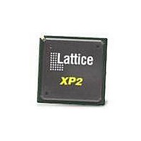
LFXP2-8E-7FT256C Lattice, LFXP2-8E-7FT256C Datasheet - Page 311

LFXP2-8E-7FT256C
Manufacturer Part Number
LFXP2-8E-7FT256C
Description
FPGA - Field Programmable Gate Array 8K LUTs 201I/O Inst- on DSP 1.2V -7 Spd
Manufacturer
Lattice
Datasheet
1.LFXP2-8E-5FTN256I.pdf
(341 pages)
Specifications of LFXP2-8E-7FT256C
Number Of Macrocells
8000
Number Of Programmable I/os
201
Data Ram Size
226304
Supply Voltage (max)
1.26 V
Maximum Operating Temperature
+ 85 C
Minimum Operating Temperature
0 C
Mounting Style
SMD/SMT
Supply Voltage (min)
1.14 V
Package / Case
FTBGA-256
Lead Free Status / RoHS Status
Lead free / RoHS Compliant
Available stocks
Company
Part Number
Manufacturer
Quantity
Price
Company:
Part Number:
LFXP2-8E-7FT256C
Manufacturer:
Lattice Semiconductor Corporation
Quantity:
10 000
- Current page: 311 of 341
- Download datasheet (10Mb)
Lattice Semiconductor
SEDCLKIN
Clock input to the SED hardware.
When external SPI configuration is used, this clock is derived from the LatticeXP2’s on-chip oscillator. The on-chip
oscillator’s output goes through a divider to create MCCLK. MCCLK goes through another divider to create SED-
CLKIN.
The software default for MCCLK is 2.5 MHz, but this can be modified using the MCCLK_FREQ global preference in
ispLEVER’s pre-map Design Planner (see TN1141,
MCCLK). It has a range of 2.5 MHz to 66 MHz.
The divider for SEDCLKIN can be set to 1, 2, 4, 8, 16 or 32. The default is 1, so the default SEDCLKIN frequency is
2.5 MHz. The divider value can be set using a parameter, see the example code at the end of this document.
If internal Flash configuration mode is used, SEDCLKIN can only be set to 3.1 MHz with a divider setting of 1.
Note that SEDCLKIN is an internally generated signal, so it should not be included as an input in the user design.
See the examples at the end of this document. Also note that while inputs to the SED block are clocked using SED-
CLKIN, no attempt has been made to synchronize between clock domains. If this is a concern for a particular
design then the designer will need to provide synchronization.
OSC_DIV
Options: 1, 2, 4, 8, 16 or 32 for external configuration. Only 1 can be selected for internal configuration. The CLK
that drives the SED module will be set by MCCLK/OSC_DIV.
SEDENABLE
Level-sensitive signal which starts SED checking.
Table 16-2. SEDENABLE
SEDCLKOUT
Gated version of SEDCLKIN, SEDCLKOUT is gated by SEDENABLE.
SEDSTART
Active high input to the SED hardware, sampled on the rising edge of SEDCLKIN.
Table 16-3. SEDSTART
SEDFRCERRN
Active high input to the SED hardware, sampled on the rising edge of SEDCLKIN.
Table 16-4. SEDFRCERRN
State
State
State
1
0
1
0
Enables output of SEDCLKOUT, arms SED hardware.
Start error detection. Must be high a minimum of one SEDCLKIN period.
No action.
No action.
Forces SEDERR high, simulating an SED error.
LatticeXP2 sysCONFIG Usage Guide
16-3
Description
Description
Description
Detection Usage Guide
LatticeXP2 Soft Error
for supported values of
Related parts for LFXP2-8E-7FT256C
Image
Part Number
Description
Manufacturer
Datasheet
Request
R

Part Number:
Description:
FPGA - Field Programmable Gate Array 8K LUTs 201 I/O Inst on DSP 1.2V -5 Spd
Manufacturer:
Lattice
Datasheet:

Part Number:
Description:
FPGA - Field Programmable Gate Array 8K LUTs 201I/O Inst- on DSP 1.2V -5 Spd
Manufacturer:
Lattice
Datasheet:

Part Number:
Description:
FPGA - Field Programmable Gate Array 8K LUTs 100 I/O Inst on DSP 1.2V -5 Spd
Manufacturer:
Lattice
Datasheet:

Part Number:
Description:
FPGA - Field Programmable Gate Array 8K LUTs 100I/O Inst- on DSP 1.2V -5 Spd
Manufacturer:
Lattice
Datasheet:

Part Number:
Description:
IC, LATTICEXP2 FPGA, 435MHZ, QFP-208
Manufacturer:
LATTICE SEMICONDUCTOR
Datasheet:
Part Number:
Description:
FPGA LatticeXP2 Family 8000 Cells Flash Technology 1.2V 144-Pin TQFP
Manufacturer:
LATTICE SEMICONDUCTOR
Datasheet:

Part Number:
Description:
IC DSP 8KLUTS 146I/O 208PQFP
Manufacturer:
Lattice
Datasheet:

Part Number:
Description:
IC DSP 8KLUTS 100I/O 144TQFP
Manufacturer:
Lattice
Datasheet:

Part Number:
Description:
IC DSP 8KLUTS 86I/O 132CSBGA
Manufacturer:
Lattice
Datasheet:

Part Number:
Description:
IC DSP 8KLUTS 86I/O 132CSBGA
Manufacturer:
Lattice
Datasheet:

Part Number:
Description:
IC DSP 8KLUTS 146I/O 208PQFP
Manufacturer:
Lattice
Datasheet:

Part Number:
Description:
IC DSP 8KLUTS 201I/O 256FTBGA
Manufacturer:
Lattice
Datasheet:

Part Number:
Description:
IC FPGA 8KLUTS 86I/O 132-BGA
Manufacturer:
Lattice
Datasheet:

Part Number:
Description:
IC FPGA 8KLUTS 86I/O 132-BGA
Manufacturer:
Lattice
Datasheet:

Part Number:
Description:
IC FPGA 8KLUTS 201I/O 256-BGA
Manufacturer:
Lattice
Datasheet:


