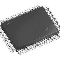
LFEC3E-3QN208C Lattice, LFEC3E-3QN208C Datasheet - Page 9

LFEC3E-3QN208C
Manufacturer Part Number
LFEC3E-3QN208C
Description
FPGA - Field Programmable Gate Array 3.1K LUTs
Manufacturer
Lattice
Datasheet
1.LFEC3E-5TN144C.pdf
(163 pages)
Specifications of LFEC3E-3QN208C
Number Of Macrocells
3100
Number Of Programmable I/os
145
Data Ram Size
56320
Supply Voltage (max)
1.26 V
Maximum Operating Temperature
+ 100 C
Minimum Operating Temperature
- 40 C
Mounting Style
SMD/SMT
Supply Voltage (min)
1.14 V
Package / Case
PQFP-208
Lead Free Status / RoHS Status
Lead free / RoHS Compliant
Available stocks
Company
Part Number
Manufacturer
Quantity
Price
Company:
Part Number:
LFEC3E-3QN208C
Manufacturer:
Lattice
Quantity:
135
Company:
Part Number:
LFEC3E-3QN208C
Manufacturer:
Lattice Semiconductor Corporation
Quantity:
10 000
Part Number:
LFEC3E-3QN208C
Manufacturer:
LATTICE
Quantity:
20 000
- Current page: 9 of 163
- Download datasheet (962Kb)
Lattice Semiconductor
Figure 2-5. Distributed Memory Primitives
ROM Mode: The ROM mode uses the same principal as the RAM modes, but without the Write port. Pre-loading is
accomplished through the programming interface during configuration.
PFU Modes of Operation
Slices can be combined within a PFU to form larger functions. Table 2-4 tabulates these modes and documents the
functionality possible at the PFU level.
Table 2-4. PFU Modes of Operation
1. These modes are not available in PFF blocks
MUX 16x1 x 1
MUX 2x1 x 8
MUX 4x1 x 4
MUX 8x1 x 2
LUT 6x 2 or
LUT 4x8 or
LUT 5x4 or
LUT 7x1 or
WRE
Logic
AD0
AD1
AD2
AD3
AD0
AD1
AD2
AD3
DI0
DI1
CK
ROM16x1
SPR16x2
2-bit Counter x 4
2-bit Comp x 4
2-bit Add x 4
2-bit Sub x 4
Ripple
DO0
DO0
DO1
2-6
DPR16x2 x 2
DPR16x4 x 1
SPR16x2 x 4
SPR16x4 x 2
SPR16x8 x 1
WAD0
WAD1
WAD2
WAD3
WCK
WRE
RAM
DI0
DI1
1
LatticeECP/EC Family Data Sheet
DPR16x2
ROM16x1 x 8
ROM16x2 x 4
ROM16x4 x 2
ROM16x8 x 1
ROM
RAD0
RAD1
RAD2
RAD3
RDO0
RDO1
WDO0
WDO1
Architecture
Related parts for LFEC3E-3QN208C
Image
Part Number
Description
Manufacturer
Datasheet
Request
R

Part Number:
Description:
FPGA - Field Programmable Gate Array 3.1K LUTs 97 IO 1.2V -3 Spd I
Manufacturer:
Lattice

Part Number:
Description:
FPGA - Field Programmable Gate Array 3.1K LUTs 67 IO 1.2V -3 Spd I
Manufacturer:
Lattice

Part Number:
Description:
FPGA - Field Programmable Gate Array 3.1K LUTs 145 IO 1.2 V -3 Spd I
Manufacturer:
Lattice
Part Number:
Description:
FPGA LatticeEC Family 3100 Cells 340MHz 130nm (CMOS) Technology 1.2V 256-Pin FBGA
Manufacturer:
LATTICE SEMICONDUCTOR
Datasheet:

Part Number:
Description:
FPGA - Field Programmable Gate Array 3.1K LUTs Pb-Free
Manufacturer:
Lattice
Datasheet:

Part Number:
Description:
FPGA LatticeEC Family 3100 Cells 340MHz 130nm (CMOS) Technology 1.2V 256-Pin FBGA
Manufacturer:
Lattice
Datasheet:

Part Number:
Description:
IC FPGA 3.1KLUTS 67I/O 100-TQFP
Manufacturer:
Lattice
Datasheet:

Part Number:
Description:
IC FPGA 3.1KLUTS 97I/O 144-TQFP
Manufacturer:
Lattice
Datasheet:

Part Number:
Description:
IC FPGA 3.1KLUTS 97I/O 144-TQFP
Manufacturer:
Lattice
Datasheet:

Part Number:
Description:
IC FPGA 3.1KLUTS 160I/O 256-BGA
Manufacturer:
Lattice
Datasheet:

Part Number:
Description:
IC FPGA 3.1KLUTS 67I/O 100-TQFP
Manufacturer:
Lattice
Datasheet:

Part Number:
Description:
IC FPGA 3.1KLUTS 145I/O 208-PQFP
Manufacturer:
Lattice
Datasheet:

Part Number:
Description:
IC FPGA 3KLUTS 208PQFP
Manufacturer:
Lattice
Datasheet:

Part Number:
Description:
IC FPGA 3.1KLUTS 160I/O 256-BGA
Manufacturer:
Lattice
Datasheet:

Part Number:
Description:
IC FPGA 3.1KLUTS 160I/O 256-BGA
Manufacturer:
Lattice
Datasheet:


