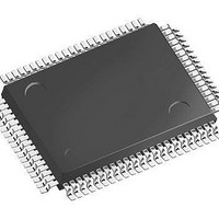
LFEC3E-3QN208C Lattice, LFEC3E-3QN208C Datasheet - Page 69

LFEC3E-3QN208C
Manufacturer Part Number
LFEC3E-3QN208C
Description
FPGA - Field Programmable Gate Array 3.1K LUTs
Manufacturer
Lattice
Datasheet
1.LFEC3E-5TN144C.pdf
(163 pages)
Specifications of LFEC3E-3QN208C
Number Of Macrocells
3100
Number Of Programmable I/os
145
Data Ram Size
56320
Supply Voltage (max)
1.26 V
Maximum Operating Temperature
+ 100 C
Minimum Operating Temperature
- 40 C
Mounting Style
SMD/SMT
Supply Voltage (min)
1.14 V
Package / Case
PQFP-208
Lead Free Status / RoHS Status
Lead free / RoHS Compliant
Available stocks
Company
Part Number
Manufacturer
Quantity
Price
Company:
Part Number:
LFEC3E-3QN208C
Manufacturer:
Lattice
Quantity:
135
Company:
Part Number:
LFEC3E-3QN208C
Manufacturer:
Lattice Semiconductor Corporation
Quantity:
10 000
Part Number:
LFEC3E-3QN208C
Manufacturer:
LATTICE
Quantity:
20 000
- Current page: 69 of 163
- Download datasheet (962Kb)
Lattice Semiconductor
PICs and DDR Data (DQ) Pins Associated with the DDR Strobe (DQS) Pin
P[Edge] [n-4]
P[Edge] [n-3]
P[Edge] [n-2]
P[Edge] [n-1]
P[Edge] [n]
P[Edge] [n+1]
P[Edge] [n+2]
P[Edge] [n+3]
Notes:
1. “n” is a Row/Column PIC number
2. The DDR interface is designed for memories that support one DQS strobe per eight bits of
3. PIC numbering definitions are provided in the “Signal Names” column of the Signal Descrip-
data. In some packages, all the potential DDR data (DQ) pins may not be available.
tions table.
PICs Associated
with DQS Strobe
PIO Within PIC
4-3
A
B
A
B
A
B
A
B
A
B
A
B
A
B
A
B
LatticeECP/EC Family Data Sheet
DDR Strobe (DQS) and
Data (DQ) Pins
[Edge]DQSn
DQ
DQ
DQ
DQ
DQ
DQ
DQ
DQ
DQ
DQ
DQ
DQ
DQ
DQ
DQ
Pinout Information
Related parts for LFEC3E-3QN208C
Image
Part Number
Description
Manufacturer
Datasheet
Request
R

Part Number:
Description:
FPGA - Field Programmable Gate Array 3.1K LUTs 97 IO 1.2V -3 Spd I
Manufacturer:
Lattice

Part Number:
Description:
FPGA - Field Programmable Gate Array 3.1K LUTs 67 IO 1.2V -3 Spd I
Manufacturer:
Lattice

Part Number:
Description:
FPGA - Field Programmable Gate Array 3.1K LUTs 145 IO 1.2 V -3 Spd I
Manufacturer:
Lattice
Part Number:
Description:
FPGA LatticeEC Family 3100 Cells 340MHz 130nm (CMOS) Technology 1.2V 256-Pin FBGA
Manufacturer:
LATTICE SEMICONDUCTOR
Datasheet:

Part Number:
Description:
FPGA - Field Programmable Gate Array 3.1K LUTs Pb-Free
Manufacturer:
Lattice
Datasheet:

Part Number:
Description:
FPGA LatticeEC Family 3100 Cells 340MHz 130nm (CMOS) Technology 1.2V 256-Pin FBGA
Manufacturer:
Lattice
Datasheet:

Part Number:
Description:
IC FPGA 3.1KLUTS 67I/O 100-TQFP
Manufacturer:
Lattice
Datasheet:

Part Number:
Description:
IC FPGA 3.1KLUTS 97I/O 144-TQFP
Manufacturer:
Lattice
Datasheet:

Part Number:
Description:
IC FPGA 3.1KLUTS 97I/O 144-TQFP
Manufacturer:
Lattice
Datasheet:

Part Number:
Description:
IC FPGA 3.1KLUTS 160I/O 256-BGA
Manufacturer:
Lattice
Datasheet:

Part Number:
Description:
IC FPGA 3.1KLUTS 67I/O 100-TQFP
Manufacturer:
Lattice
Datasheet:

Part Number:
Description:
IC FPGA 3.1KLUTS 145I/O 208-PQFP
Manufacturer:
Lattice
Datasheet:

Part Number:
Description:
IC FPGA 3KLUTS 208PQFP
Manufacturer:
Lattice
Datasheet:

Part Number:
Description:
IC FPGA 3.1KLUTS 160I/O 256-BGA
Manufacturer:
Lattice
Datasheet:

Part Number:
Description:
IC FPGA 3.1KLUTS 160I/O 256-BGA
Manufacturer:
Lattice
Datasheet:


