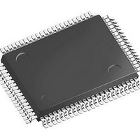
LFEC3E-3QN208C Lattice, LFEC3E-3QN208C Datasheet - Page 19

LFEC3E-3QN208C
Manufacturer Part Number
LFEC3E-3QN208C
Description
FPGA - Field Programmable Gate Array 3.1K LUTs
Manufacturer
Lattice
Datasheet
1.LFEC3E-5TN144C.pdf
(163 pages)
Specifications of LFEC3E-3QN208C
Number Of Macrocells
3100
Number Of Programmable I/os
145
Data Ram Size
56320
Supply Voltage (max)
1.26 V
Maximum Operating Temperature
+ 100 C
Minimum Operating Temperature
- 40 C
Mounting Style
SMD/SMT
Supply Voltage (min)
1.14 V
Package / Case
PQFP-208
Lead Free Status / RoHS Status
Lead free / RoHS Compliant
Available stocks
Company
Part Number
Manufacturer
Quantity
Price
Company:
Part Number:
LFEC3E-3QN208C
Manufacturer:
Lattice
Quantity:
135
Company:
Part Number:
LFEC3E-3QN208C
Manufacturer:
Lattice Semiconductor Corporation
Quantity:
10 000
Part Number:
LFEC3E-3QN208C
Manufacturer:
LATTICE
Quantity:
20 000
- Current page: 19 of 163
- Download datasheet (962Kb)
Lattice Semiconductor
Table 2-7. Maximum Number of Elements in a Block
Some options are available in four elements. The input register in all the elements can be directly loaded or can be
loaded as shift registers from previous operand registers. In addition by selecting “dynamic operation” in the
‘Signed/Unsigned’ options the operands can be switched between signed and unsigned on every cycle. Similarly
by selecting ‘Dynamic operation’ in the ‘Add/Sub’ option the Accumulator can be switched between addition and
subtraction on every cycle.
MULT sysDSP Element
This multiplier element implements a multiply with no addition or accumulator nodes. The two operands, A and B,
are multiplied and the result is available at the output. The user can enable the input/output and pipeline registers.
Figure 2-19 shows the MULT sysDSP element.
Figure 2-19. MULT sysDSP Element
MAC sysDSP Element
In this case the two operands, A and B, are multiplied and the result is added with the previous accumulated value.
This accumulated value is available at the output. The user can enable the input and pipeline registers but the out-
put register is always enabled. The output register is used to store the accumulated value. A registered overflow
signal is also available. The overflow conditions are provided later in this document. Figure 2-20 shows the MAC
sysDSP element.
MULT
MAC
MULTADD
MULTADDSUM
Width of Multiply
Multiplicand
Multiplier
Signed
Shift Register B Out
Shift Register B In
n
Input Data
Register B
n
n
n
Register
Input
m
x9
8
2
4
2
Register A
Input Data
m
m
Shift Register A Out
m
Shift Register A In
2-16
Multiplier
m
n
To
Multiplier
x18
Register
Pipeline
x
4
2
2
1
CLK (CLK0,CLK1,CLK2,CLK3)
CE (CE0,CE1,CE2,CE3)
RST(RST0,RST1,RST2,RST3)
LatticeECP/EC Family Data Sheet
(default)
m+n
m+n
x36
—
—
—
1
Output
Architecture
Related parts for LFEC3E-3QN208C
Image
Part Number
Description
Manufacturer
Datasheet
Request
R

Part Number:
Description:
FPGA - Field Programmable Gate Array 3.1K LUTs 97 IO 1.2V -3 Spd I
Manufacturer:
Lattice

Part Number:
Description:
FPGA - Field Programmable Gate Array 3.1K LUTs 67 IO 1.2V -3 Spd I
Manufacturer:
Lattice

Part Number:
Description:
FPGA - Field Programmable Gate Array 3.1K LUTs 145 IO 1.2 V -3 Spd I
Manufacturer:
Lattice
Part Number:
Description:
FPGA LatticeEC Family 3100 Cells 340MHz 130nm (CMOS) Technology 1.2V 256-Pin FBGA
Manufacturer:
LATTICE SEMICONDUCTOR
Datasheet:

Part Number:
Description:
FPGA - Field Programmable Gate Array 3.1K LUTs Pb-Free
Manufacturer:
Lattice
Datasheet:

Part Number:
Description:
FPGA LatticeEC Family 3100 Cells 340MHz 130nm (CMOS) Technology 1.2V 256-Pin FBGA
Manufacturer:
Lattice
Datasheet:

Part Number:
Description:
IC FPGA 3.1KLUTS 67I/O 100-TQFP
Manufacturer:
Lattice
Datasheet:

Part Number:
Description:
IC FPGA 3.1KLUTS 97I/O 144-TQFP
Manufacturer:
Lattice
Datasheet:

Part Number:
Description:
IC FPGA 3.1KLUTS 97I/O 144-TQFP
Manufacturer:
Lattice
Datasheet:

Part Number:
Description:
IC FPGA 3.1KLUTS 160I/O 256-BGA
Manufacturer:
Lattice
Datasheet:

Part Number:
Description:
IC FPGA 3.1KLUTS 67I/O 100-TQFP
Manufacturer:
Lattice
Datasheet:

Part Number:
Description:
IC FPGA 3.1KLUTS 145I/O 208-PQFP
Manufacturer:
Lattice
Datasheet:

Part Number:
Description:
IC FPGA 3KLUTS 208PQFP
Manufacturer:
Lattice
Datasheet:

Part Number:
Description:
IC FPGA 3.1KLUTS 160I/O 256-BGA
Manufacturer:
Lattice
Datasheet:

Part Number:
Description:
IC FPGA 3.1KLUTS 160I/O 256-BGA
Manufacturer:
Lattice
Datasheet:


