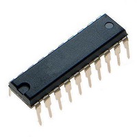
ATTINY861-20PU Atmel, ATTINY861-20PU Datasheet - Page 183

ATTINY861-20PU
Manufacturer Part Number
ATTINY861-20PU
Description
Microcontrollers (MCU) 8kB Flash 0.512kB EEPROM 16 I/O Pins
Manufacturer
Atmel
Specifications of ATTINY861-20PU
Processor Series
ATTINY8x
Core
AVR8
Data Bus Width
8 bit
Data Ram Size
512 B
Interface Type
2-Wire/SPI/USI
Maximum Clock Frequency
20 MHz
Number Of Programmable I/os
16
Number Of Timers
2
Operating Supply Voltage
2.7 V to 5.5 V
Maximum Operating Temperature
+ 85 C
Mounting Style
Through Hole
3rd Party Development Tools
EWAVR, EWAVR-BL
Development Tools By Supplier
ATAVRDRAGON, ATSTK500, ATSTK600, ATAVRISP2, ATAVRONEKIT, ATAVRMC320
Minimum Operating Temperature
- 40 C
On-chip Adc
11-ch x 10-bit
Program Memory Type
Flash
Program Memory Size
8 KB
Package / Case
PDIP-20
Controller Family/series
AVR Tiny
Core Size
8 Bit
No. Of I/o's
16
Eeprom Memory Size
512Byte
Ram Memory Size
512Byte
Cpu Speed
20MHz
No. Of Timers
2
Rohs Compliant
Yes
Package
20PDIP
Device Core
AVR
Family Name
ATtiny
Maximum Speed
20 MHz
Ram Size
512 Byte
Operating Temperature
-40 to 85 °C
Lead Free Status / RoHS Status
Lead free / RoHS Compliant
Available stocks
Company
Part Number
Manufacturer
Quantity
Price
Company:
Part Number:
ATTINY861-20PU
Manufacturer:
Atmel
Quantity:
135
Company:
Part Number:
ATTINY861-20PU ES
Manufacturer:
ATMEL
Quantity:
215
- Current page: 183 of 242
- Download datasheet (5Mb)
18.7.7
2588E–AVR–08/10
Reading the Flash
programmed simultaneously. The programming algorithm for the EEPROM data memory is as
follows (refer to
Data loading):
Figure 18-6. Programming the EEPROM Waveforms
The algorithm for reading the Flash memory is as follows (refer to
page 180
RESET +12V
1. A: Load Command “0001 0001”.
2. G: Load Address High Byte (0x00 - 0xFF).
3. B: Load Address Low Byte (0x00 - 0xFF).
4. C: Load Data (0x00 - 0xFF).
5. E: Latch data (give PAGEL a positive pulse).
6. K: Repeat 3 through 5 until the entire buffer is filled.
7. L: Program EEPROM page
1. A: Load Command “0000 0010”.
2. G: Load Address High Byte (0x00 - 0xFF).
3. B: Load Address Low Byte (0x00 - 0xFF).
4. Set OE to “0”, and BS1 to “0”. The Flash word low byte can now be read at DATA.
5. Set BS to “1”. The Flash word high byte can now be read at DATA.
6. Set OE to “1”.
PAGEL/BS1
RDY/BSY
XA1/BS2
XTAL1
DATA
a. Set BS to “0”.
b. Give WR a negative pulse. This starts programming of the EEPROM page.
c. Wait until to RDY/BSY goes high before programming the next page (See
XA0
WR
OE
RDY/BSY goes low.
18-6
for details on Command and Address loading):
for signal waveforms).
0x11
A
“Programming the Flash” on page 180
ADDR. HIGH
G
ADDR. LOW
B
DATA
C
XX
E
ADDR. LOW
B
for details on Command, Address and
DATA
C
K
XX
E
“Programming the Flash” on
L
Figure
183
Related parts for ATTINY861-20PU
Image
Part Number
Description
Manufacturer
Datasheet
Request
R

Part Number:
Description:
Manufacturer:
Atmel Corporation
Datasheet:

Part Number:
Description:
Manufacturer:
Atmel Corporation
Datasheet:

Part Number:
Description:
IC MCU AVR 8K FLASH 20MHZ 32-QFN
Manufacturer:
Atmel
Datasheet:

Part Number:
Description:
IC MCU AVR 8K FLASH 20MHZ 20SOIC
Manufacturer:
Atmel
Datasheet:

Part Number:
Description:
MCU AVR 8K FLASH 15MHZ 32-QFN
Manufacturer:
Atmel
Datasheet:

Part Number:
Description:
MCU AVR 8K FLASH 15MHZ 20-SOIC
Manufacturer:
Atmel
Datasheet:

Part Number:
Description:
MCU AVR 8KB FLASH 15MHZ 32-VQFN
Manufacturer:
Atmel
Datasheet:

Part Number:
Description:
8-bit Microcontrollers - MCU 8KB FL 512B EE 512B SRAM 20MHZ IND 5V
Manufacturer:
Atmel

Part Number:
Description:
IC, MCU, 8BIT, 2K FLASH, 20SOIC
Manufacturer:
Atmel
Datasheet:

Part Number:
Description:
IC, MCU, 8BIT, 2K FLASH, 20PDIP
Manufacturer:
Atmel
Datasheet:


