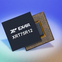
XRT75R12IB-F Exar Corporation, XRT75R12IB-F Datasheet - Page 42

XRT75R12IB-F
Manufacturer Part Number
XRT75R12IB-F
Description
Peripheral Drivers & Components (PCIs) 12 Channel 3.3V-5V temp -45 to 85C
Manufacturer
Exar Corporation
Datasheet
1.XRT75R12IB-F.pdf
(90 pages)
Specifications of XRT75R12IB-F
Maximum Operating Temperature
+ 85 C
Minimum Operating Temperature
- 40 C
Mounting Style
SMD/SMT
Operating Supply Voltage
3.3 V
Package / Case
TBGA-420
Ic Interface Type
Parallel, Serial
Supply Voltage Range
3.135V To 3.465V
Operating Temperature Range
-40°C To +85°C
Digital Ic Case Style
BGA
No. Of Pins
420
Filter Terminals
SMD
Rohs Compliant
Yes
Data Rate Max
51.84Mbps
Lead Free Status / RoHS Status
Lead free / RoHS Compliant
XRT75R12
TWELVE CHANNEL E3/DS3/STS-1 LINE INTERFACE UNIT WITH JITTER ATTENUATOR
Jitter Transfer function is defined as the ratio of jitter on the output relative to the jitter applied on the input
versus frequency. There are two distinct characteristics in jitter transfer, jitter gain (jitter peaking) defined as
the highest ratio above 0dB and jitter transfer bandwidth. The overall jitter transfer bandwidth is controlled by a
low bandwidth loop, typically using a voltage-controlled crystal oscillator (VCXO).
The jitter transfer function is a ratio between the jitter output and jitter input for a component, or system often
expressed in dB. A negative dB jitter transfer indicates the element removed jitter. A positive dB jitter transfer
indicates the element added jitter. A zero dB jitter transfer indicates the element had no effect on jitter.
Table 11
N
An advanced crystal-less jitter attenuator per channel is included in the XRT75R12. The jitter attenuator
requires no external crystal nor high-frequency reference clock. By clearing or setting the JATx/Rx_n bits in
the channel control registers selects the jitter attenuator either in the Receive or Transmit path on per channel
basis. The FIFO size can be either 16-bit or 32-bit. The bits JA0_n and JA1_n can be set to appropriate
combination to select the different FIFO sizes or to disable the Jitter Attenuator on a per channel basis. Data is
clocked into the FIFO with the associated clock signal (TxClk or RxClk) and clocked out of the FIFO with the
dejittered clock. When the FIFO is within two bits of overflowing or underflowing, the FIFO limit status bit, FL_n
is set to “1” in the Alarm status register. Reading this bit clears the FIFO and resets the bit into default state.
N
5.2
5.3
OTE
OTE
B
34368
44736
44736
51840
IT
(
KB
: The above specifications can be met only with a jitter attenuator that supports E3/DS3/STS-1 rates.
: It is recommended to select the 16-bit FIFO for delay-sensitive applications as well as for removing smaller amounts
R
/
of jitter.
ATE
S
J
Jitter Attenuator
)
ITTER
shows the jitter transfer characteristics and/or jitter attenuation specifications for various data rates:
ETSI TBR-24
T
CORE Cat II
CORE Cat II
ITU-T G.823
Table 12
CORE Cat I
ABLE
S
T
GR-499
GR-499
GR-253
RANSFER
TANDARD
E3
10: J
specifies the jitter transfer mask requirements for various data rates:
ITTER
T
I
ABLE
NPUT
1.5
A1
10
15
A
5
MPLITUDE VERSUS
J
11: J
ITTER
ITTER
A
0.15
0.1
0.3
1.5
A2
MPLITUDE
GR-499 CORE section 7.3.2
Category I and Category II
T
RANSFER
(UI
M
0.15
A3
-
-
-
ODULATION
DS3
39
P
-
P
S
)
PECIFICATION
F
1(H
100
10
10
10
F
Z
REQUENCY
)
/R
F
1000
2(H
2.3k
EFERENCES
669
30
M
ODULATION
Z
)
(J
GR-253 CORE section 5.6.2.1
ITTER
F
3(
22.3
300
10
60
K
T
H
F
OLERANCE
Z
REQUENCY
)
STS-1
F
4(
800
300
300
K
2
H
)
Z
)
REV. 1.0.4
F
5(
20
K
-
-
-
H
Z
)


