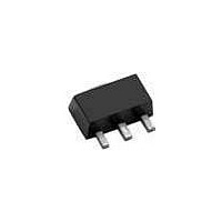
TP2510N8-G Supertex, TP2510N8-G Datasheet - Page 2

TP2510N8-G
Manufacturer Part Number
TP2510N8-G
Description
MOSFET Small Signal 100V 3.5Ohm
Manufacturer
Supertex
Type
Power MOSFETr
Datasheet
1.TP2510N8-G.pdf
(5 pages)
Specifications of TP2510N8-G
Minimum Operating Temperature
- 55 C
Configuration
Single
Transistor Polarity
P-Channel
Resistance Drain-source Rds (on)
3.5 Ohm @ 10 V
Drain-source Breakdown Voltage
100 V
Gate-source Breakdown Voltage
+/- 20 V
Continuous Drain Current
0.48 A
Power Dissipation
1600 mW
Maximum Operating Temperature
+ 150 C
Mounting Style
SMD/SMT
Package / Case
SOT-89
Number Of Elements
1
Polarity
P
Channel Mode
Enhancement
Drain-source On-res
3.5Ohm
Drain-source On-volt
100V
Gate-source Voltage (max)
±20V
Drain Current (max)
480mA
Output Power (max)
Not RequiredW
Frequency (max)
Not RequiredMHz
Noise Figure
Not RequireddB
Power Gain
Not RequireddB
Drain Efficiency
Not Required%
Operating Temp Range
-55C to 150C
Operating Temperature Classification
Military
Mounting
Surface Mount
Pin Count
3 +Tab
Package Type
SOT-89
Lead Free Status / RoHS Status
Lead free / RoHS Compliant
Available stocks
Company
Part Number
Manufacturer
Quantity
Price
Company:
Part Number:
TP2510N8-G
Manufacturer:
MICROCHIP
Quantity:
12 000
† I
‡ Mounted on FR5 board, 25mm x 25mm x 1.57mm.
Thermal Characteristics
Electrical Characteristics
Notes:
Switching Waveforms and Test Circuit
TO-243AA
1.
2.
D
∆R
Package
∆V
R
BV
(continuous) is limited by max rated T
V
Sym
t
I
C
C
t
OUTPUT
C
d(OFF)
I
I
G
V
D(ON)
DS(ON)
d(ON)
GS(th)
GSS
DSS
DS(ON)
t
OSS
GS(th)
RSS
t
t
INPUT
ISS
SD
rr
All D.C. parameters 100% tested at 25°C unless otherwise stated. (Pulse test: 300µs pulse, 2% duty cycle.)
All A.C. parameters sample tested.
FS
r
f
DSS
-10V
V
0V
0V
DD
Parameter
Drain-to-source breakdown voltage
Gate threshold voltage
Change in V
Gate body leakage
Zero gate voltage drain current
On-state drain current
Static drain-to-source on-state resistance
Change in R
Forward transconductance
Input capacitance
Common source output capacitance
Reverse transfer capacitance
Turn-on delay time
Rise time
Turn-off delay time
Fall time
Diode forward voltage drop
Reverse recovery time
10%
(continuous)
-480
(mA)
I
D
t
d(ON)
GS(th)
DS(ON)
10%
t
(ON)
†
with temperature
with temperature
t
r
j
.
●
90%
1235 Bordeaux Drive, Sunnyvale, CA 94089
(pulsed)
-2.5
(T
(A)
I
A
D
= 25°C unless otherwise specified )
90%
t
d(OFF)
t
90%
(OFF)
Power Dissipation
t
F
10%
@ T
1.6
A
(W)
= 25
-100
‡
Min
-1.0
-0.4
-1.5
300
2
-
-
-
-
-
-
-
-
-
-
-
-
-
-
O
C
Typ
-0.6
-2.5
360
300
5.0
2.0
80
40
10
-
-
-
-
-
-
-
-
-
-
-
-
GENERATOR
PULSE
●
(
O
C/W)
Tel: 408-222-8888
θ
15
-100
Max
-2.4
-1.0
-1.8
125
jc
5.0
-10
7.0
3.5
1.7
70
25
10
15
20
15
INPUT
-
-
-
-
-
R
GEN
mV/
mmho
Units
%/
mA
μA
nA
pF
ns
ns
Ω
V
V
A
V
(
O
O
O
78
C
C/W)
θ
C
ja
‡
●
Conditions
V
V
V
V
V
V
V
V
V
V
V
V
V
V
V
f = 1.0 MHz
V
I
R
V
V
www.supertex.com
D
GS
GS
GS
GS
GS
DS
GS
GS
GS
GS
GS
GS
DS
GS
DS
DD
GS
GS
GEN
= -1.0A,
= 0.8 Max Rating,
= -25V, I
= -25V,
= 0V, I
= V
= V
= ± 20V, V
= 0V, V
= 0V, T
= -5.0V, V
= -10V, V
= -5.0V, I
= -10V, I
= -10V, I
= 0V,
= -25V,
= 0V, I
= 0V, I
= 25Ω
-480
DS
DS
(mA)
I
DR
, I
, I
†
D
SD
SD
A
D
D
DS
= -2.0mA
= -1.0mA
= -1.0mA
= 125°C
D
D
D
= -1.0A
= -1.0A
D
DS
V
= Max Rating
DS
= -750mA
= -750mA
= -750mA
R
DS
= -250mA
DD
L
= -25V
= -25V
TP2510
= 0V
D.U.T.
Output
-2.5
I
(A)
DRM


