SUD50N06-09L-E3 Vishay, SUD50N06-09L-E3 Datasheet - Page 2
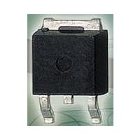
SUD50N06-09L-E3
Manufacturer Part Number
SUD50N06-09L-E3
Description
MOSFET Power 60V 50A 136W 9.3mohm @ 10V
Manufacturer
Vishay
Datasheet
1.SUD50N06-09L-E3.pdf
(6 pages)
Specifications of SUD50N06-09L-E3
Transistor Polarity
N-Channel
Minimum Operating Temperature
- 55 C
Configuration
Single
Resistance Drain-source Rds (on)
0.0093 Ohm @ 10 V
Drain-source Breakdown Voltage
60 V
Gate-source Breakdown Voltage
+/- 20 V
Continuous Drain Current
50 A
Power Dissipation
8300 mW
Maximum Operating Temperature
+ 175 C
Mounting Style
SMD/SMT
Package / Case
TO-252
Continuous Drain Current Id
50A
Drain Source Voltage Vds
60V
On Resistance Rds(on)
12.2mohm
Rds(on) Test Voltage Vgs
10V
Threshold Voltage Vgs Typ
2V
Lead Free Status / RoHS Status
Lead free / RoHS Compliant
Lead Free Status / RoHS Status
Lead free / RoHS Compliant, Lead free / RoHS Compliant
Available stocks
Company
Part Number
Manufacturer
Quantity
Price

Part Number:
SUD50N06-09L-E3
Manufacturer:
V1SHAY
Quantity:
20 000


SUD50N06-09L
Vishay Siliconix
Notes:
a. For design aid only; not subject to production testing.
b. Pulse test; pulse width ≤ 300 µs, duty cycle ≤ 2 %.
c. Independent of operating temperature.
Stresses beyond those listed under “Absolute Maximum Ratings” may cause permanent damage to the device. These are stress ratings only, and functional operation
of the device at these or any other conditions beyond those indicated in the operational sections of the specifications is not implied. Exposure to absolute maximum
rating conditions for extended periods may affect device reliability.
www.vishay.com
2
SPECIFICATIONS T
Parameter
Static
Drain-Source Breakdown Voltage
Gate Threshold Voltage
Gate-Body Leakage
Zero Gate Voltage Drain Current
On-State Drain Current
Drain-Source On-State Resistance
Forward Transconductance
Dynamic
Input Capacitance
Output Capacitance
Reverse Transfer Capacitance
Total Gate Charge
Gate-Source Charge
Gate-Drain Charge
Turn-On Delay Time
Rise Time
Turn-Off Delay Time
Fall Time
Source-Drain Diode Ratings and Characteristics (T
Pulsed Current
Diode Forward Voltage
Reverse Recovery Time
c
c
c
c
c
c
c
b
b
J
= 25 °C, unless otherwise noted
b
V
Symbol
V
r
(BR)DSS
I
DS(on)
t
t
I
C
I
C
V
GS(th)
D(on)
C
Q
Q
d(on)
d(off)
GSS
DSS
I
Q
g
SM
t
oss
t
t
rss
SD
iss
rr
fs
gs
gd
r
f
g
C
V
V
I
V
V
V
D
V
= 25 °C)
DS
DS
GS
GS
DS
GS
≅ 50 A, V
I
= 60 V, V
= 60 V, V
= 10 V, I
= 10 V, I
F
V
= 30 V, V
V
= 0 V, V
V
V
V
V
V
V
= 20 A, di/dt = 100 A/µs
DS
V
DS
DD
I
GS
DS
DS
F
GS
DS
GS
Test Conditions
= 20 A, V
= 0 V, V
= V
= 0 V, I
= 30 V, R
= 60 V, V
= 5 V, V
= 4.5 V, I
= 10 V, I
= 15 V, I
GEN
D
D
GS
DS
GS
GS
GS
= 20 A, T
= 20 A, T
, I
= 10 V, R
= 25 V, f = 1 MHz
= 0 V, T
= 0 V, T
D
= 10 V, I
GS
D
GS
GS
= 250 µA
D
D
L
GS
D
= 250 µA
= ± 20 V
= 20 A
= 20 A
= 0.6 Ω
= 10 V
= 15 A
= 0 V
= 0 V
J
J
J
J
= 125 °C
= 175 °C
g
= 125 °C
= 175 °C
D
= 2.5 Ω
= 50 A
Min
1.0
60
50
0.0074
2650
Typ
470
225
2.0
1.0
47
10
12
10
15
35
20
45
S-71660-Rev. D, 06-Aug-07
a
Document Number: 72004
0.0093
0.0122
± 100
0.016
0.020
Max
250
100
100
3.0
1.5
50
70
20
25
50
30
1
Unit
nA
µA
pF
nC
ns
ns
Ω
V
A
S
A
V
Related parts for SUD50N06-09L-E3
Image
Part Number
Description
Manufacturer
Datasheet
Request
R

Part Number:
Description:
N-Ch MOSFET DPak (TO-252) 60V 7.4mohm @ 10V
Manufacturer:
Vishay

Part Number:
Description:
N-Channel 60-V (D-S) 175 C MOSFET
Manufacturer:
VISHAY [Vishay Siliconix]
Datasheet:
Part Number:
Description:
R-C Thermal Model Parameters
Manufacturer:
VISHAY [Vishay Siliconix]
Datasheet:
Part Number:
Description:
N-Channel 60-V (D-S) 175Celsius MOSFET
Manufacturer:
VISHAY [Vishay Siliconix]
Datasheet:
Part Number:
Description:
N-Channel 60-V (D-S) 175Celsius MOSFET, Logic Level
Manufacturer:
VISHAY [Vishay Siliconix]
Datasheet:
Part Number:
Description:
N-Channel 60-V (D-S), 150 �C MOSFET
Manufacturer:
VISHAY [Vishay Siliconix]
Datasheet:
Part Number:
Description:
TRANSISTOR,MOSFET,N-CHANNEL,60V V(BR)DSS,96A I(D),TO-252
Manufacturer:
Vishay
Part Number:
Description:
TRANSISTOR,MOSFET,N-CHANNEL,60V V(BR)DSS,93A I(D),TO-252
Manufacturer:
Vishay
Part Number:
Description:
N-Channel 60-V (D-S) 175 C MOSFET
Manufacturer:
Vishay
Datasheet:
Part Number:
Description:
N-Channel 60-V (D-S) 175 C MOSFET
Manufacturer:
Vishay
Datasheet:
Part Number:
Description:
N-Channel 60-V (D-S) 150 C MOSFET
Manufacturer:
Vishay
Datasheet:
Part Number:
Description:
N-channel 60-v D-s 175 ?c Mosfet
Manufacturer:
Vishay
Datasheet:
Part Number:
Description:
N-channel 60-v Degreee Celcious Mosfet
Manufacturer:
Vishay
Datasheet: