DLP-245PB-G-CCS DLP Design Inc, DLP-245PB-G-CCS Datasheet - Page 13
DLP-245PB-G-CCS
Manufacturer Part Number
DLP-245PB-G-CCS
Description
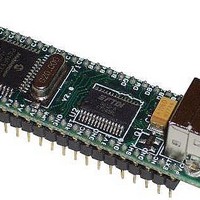
Interface Modules & Development Tools DLP-245PB-G BOARD + CCS Compiler
Manufacturer
DLP Design Inc
Datasheet
1.DLP-245PB-G.pdf
(16 pages)
Specifications of DLP-245PB-G-CCS
Interface Type
USB
Data Bus Width
8 bit
Product
Interface Modules
For Use With/related Products
16F877A
Lead Free Status / RoHS Status
Lead free / RoHS Compliant


V2.3
15
16
17
18
19
20
21
22
23
24
25
26
27
28
29
30
31
32
33
34
35
36
37
38
39
40
GROUND
SWVCC
and Q1 MOSFET power switch. R5 and C3 control the power-up rate to help limit inrush current.
GROUND
No connect
EXTVCC
PORTVCC if the module is to be powered by the USB port (typical configuration).
PORTVCC
USB port (typical configuration). 500mA is the maximum current available to the DLP-245PB-G
and target electronics if the USB device is configured for high power.
DB7
DB6
DB5
DB4
DB3
DB2
DB1
DB0
B5
B4
B0
C0
C1
C2
C3
C4
C5
C6
C7
GROUND
(I/O) Port Pin B5 connected to the 16F877A microcontroller.
(I/O) Port Pin B4 connected to the 16F877A microcontroller.
(I/O) Port Pin B0 connected to the 16F877A microcontroller.
(I/O) Port Pin C0 connected to the 16F877A microcontroller.
(I/O) Port Pin C1 connected to the 16F877A microcontroller.
(I/O) Port Pin C2 connected to the 16F877A microcontroller.
(I/O) Port Pin C3 connected to the 16F877A microcontroller.
(I/O) Port Pin C4 connected to the 16F877A microcontroller.
(I/O) Port Pin C5 connected to the 16F877A microcontroller.
(I/O) Port Pin C6 connected to the 16F877A microcontroller.
(I/O) Port Pin C7 connected to the 16F877A microcontroller.
(I/O) Line 7 of the data bus between the 16F877A and the FT245RL USB-FIFO.
(I/O) Line 6 of the data bus between the 16F877A and the FT245RL USB-FIFO.
(I/O) Line 5 of the data bus between the 16F877A and the FT245RL USB-FIFO.
(I/O) Line 4 of the data bus between the 16F877A and the FT245RL USB-FIFO.
(I/O) Line 3 of the data bus between the 16F877A and the FT245RL USB-FIFO.
(I/O) Line 2 of the data bus between the 16F877A and the FT245RL USB-FIFO.
(I/O) Line 1 of the data bus between the 16F877A and the FT245RL USB-FIFO.
(I/O) Line 0 of the data bus between the 16F877A and the FT245RL USB-FIFO.
(Out) Power from EXTVCC (Pin 19) controlled via Pin 10 (POWERN#) of the FT245RL
(In) Use for applying main power (4.4 to 5.25 volts) to the module. Connect to
(Out) Power from USB port. Connect to EXTVCC if module is to be powered by the
Page 13 of
15
February 2007
Related parts for DLP-245PB-G-CCS
Image
Part Number
Description
Manufacturer
Datasheet
Request
R

Part Number:
Description:
MODULE USB-MCU FT245RL W/16F877A
Manufacturer:
DLP Design Inc
Datasheet:

Part Number:
Description:
Interface Modules & Development Tools USB/Micro Dev Board
Manufacturer:
DLP Design Inc
Datasheet:

Part Number:
Description:
Power Supply, DIN Ral Mount, 24V, 10A, 240W, 85-264 VAC, Barrier Strip Term
Manufacturer:
TDK Corporation
Datasheet:
Part Number:
Description:
Power Supply, DIN Rail Mount, 24V, 3.70A, 89W, 110/230 VAC, NEC NFPA70 Class 2
Manufacturer:
TDK Corporation
Datasheet:

Part Number:
Description:
MODULE USB-TO-TTL SRL UART CONV
Manufacturer:
DLP Design Inc
Datasheet:

Part Number:
Description:
MODULE USB-TO-TTL PARL FIFO CONV
Manufacturer:
DLP Design Inc
Datasheet:

Part Number:
Description:
MODULE DATA-ACQUISITION 8-CH
Manufacturer:
DLP Design Inc
Datasheet:

Part Number:
Description:
MODULE DATA-ACQUISITION 20-CH
Manufacturer:
DLP Design Inc
Datasheet:

Part Number:
Description:
RFID READER/WRITER SNGL-CH OEM
Manufacturer:
DLP Design Inc
Datasheet:

Part Number:
Description:
MODULE USB-TO-FPGA TRAINING TOOL
Manufacturer:
DLP Design Inc
Datasheet:

Part Number:
Description:
MODULE USB-MCU FT232R W/18F2410
Manufacturer:
DLP Design Inc
Datasheet:

Part Number:
Description:
MODULE USB-MCU FT245RL W/SX48
Manufacturer:
DLP Design Inc
Datasheet:

Part Number:
Description:
MODULE USB-MCU FT2232D W/16F877A
Manufacturer:
DLP Design Inc
Datasheet:

Part Number:
Description:
MODULE USB-TO-FPGA SPARTAN3
Manufacturer:
DLP Design Inc
Datasheet:

Part Number:
Description:
MOD USB-MCU FT245RL W/18LF8722
Manufacturer:
DLP Design Inc
Datasheet: