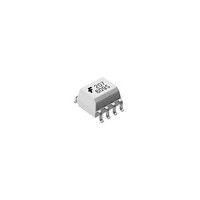
FOD2742B Fairchild Semiconductor, FOD2742B Datasheet - Page 4

FOD2742B
Manufacturer Part Number
FOD2742B
Description
Transistor Output Optocouplers Error amplifier Optocoupler
Manufacturer
Fairchild Semiconductor
Specifications of FOD2742B
Maximum Input Diode Current
20 mA
Output Device
Transistor
Output Type
DC
Configuration
1
Input Type
DC
Maximum Collector Emitter Voltage
70 V
Maximum Collector Emitter Saturation Voltage
400 mV
Isolation Voltage
2500 Vrms
Current Transfer Ratio
200 %
Maximum Forward Diode Voltage
1.5 V
Maximum Collector Current
50 mA
Maximum Power Dissipation
145 mW
Maximum Operating Temperature
+ 85 C
Minimum Operating Temperature
- 25 C
Package / Case
SOIC-8 Narrow
No. Of Channels
1
Optocoupler Output Type
Phototransistor
Input Current
10mA
Output Voltage
70V
Opto Case Style
SOIC
No. Of Pins
8
Svhc
No SVHC (15-Dec-2010)
Rohs Compliant
Yes
Lead Free Status / RoHS Status
Lead free / RoHS Compliant
Other names
FOD2742B_NL
Available stocks
Company
Part Number
Manufacturer
Quantity
Price
Part Number:
FOD2742B
Manufacturer:
FAIRCHILD/仙童
Quantity:
20 000
Company:
Part Number:
FOD2742BR2
Manufacturer:
FAIRCHIL
Quantity:
2 671
© 2003 Fairchild Semiconductor Corporation
FOD2742A
Notes
1. Device is considered as a two terminal device: Pins 1,2 3 and 4 are shorted together and Pins 5,6,7 and 8 are shorted together.
2. Common mode transient immunity at output high is the maximum tolerable (positive) dVcm/dt on the leading edge of the
OUTPUT CHARACTERISTICS
Parameter
Collector dark current
Emitter-collector voltage breakdown
Collector-emitter voltage breakdown
TRANSFER CHARACTERISTICS
Parameter
Current transfer ratio
Collector-emitter
saturation voltage
ISOLATION CHARACTERISTICS
Parameter
Input-output insulation
leakage current
Withstand insulation
voltage
Resistance (input to output)
SWITCHING CHARACTERISTICS
Parameter
Bandwidth
Common mode transient
immunity at output high
Common mode transient
immunity at output low
common mode impulse signal, Vcm, to assure that the output will remain high. Common mode transient immunity at output
low is the maximum tolerable (negative) dVcm/dt on the trailing edge of the common pulse signal,Vcm, to assure that the
output will remain low.
(RH <= 50%, T
(I
(I
LED
(RH = 45%, T
LED
(I
(I
RL = 2.2 kV (Fig. 8) (note 2)
RL = 2.2 kV (Fig. 8) (note 2)
(T
LED
LED
V
= 10 mA, Vcm = 10 V
A
I-O
= 0 mA, Vcm = 10 V
V
= 25°C Unless otherwise specified.)
(T
= 10 mA, V
= 10 mA, V
(T
I-O
= 3000 VDC) (note. 1)
(T
A
A
(V
I
A
A
= 500 VDC (note 1)
= 25°C Unless otherwise specified.)
C
FOD2742B
= 25°C Unless otherwise specified.)
V
CE
= 25°C, t = 1 min)
= 25°C Unless otherwise specified.)
= 2.5 mA) (Fig. 6)
Test Conditions
Test Conditions
Test Conditions
Test Conditions
CE
A
= 10 V) (Fig. 5)
= 25°C, t = 5s,
= 5 V) (Fig. 6)
Page 4 of 13
(I
(I
COMP
COMP
E
C
= 100 µA)
= 1.0mA)
(note 1)
(Fig. 7)
= V
= V
FB
FB,
PP
PP
,
V
Symbol
Symbol
Symbol
CMH
CML
CE (SAT)
Symbol
V
BV
BV
CTR
R
I
BW
I-O
I
ISO
I-O
CEO
ECO
CEO
OPTICALLY ISOLATED
2500
Min
ERROR AMPLIFIER
Min
Min
100
Min
70
7
10
0.16
Typ
Typ
Typ
140
1.0
1.0
50
Typ
120
10
12
1
FOD2742C
Max
Max
Max
200
0.4
1.0
Max
50
kV/µs
kV/µs
12/9/04
Vrms
Ohm
Unit
Unit
kHZ
Unit
Unit
µA
nA
%
V
V
V


